Skip to the content
4 layers200.1 × 170.2 mmFmc memory adapter, the printed circuit board in 3D

Fmc memory adapter

FlorianFrank/MemTestX1

A comprehensive test platform for advanced memory device characterization combining FPGA acceleration, real-time firmware, and automated experiment scheduling

Size
200.1 × 170.2 mm
Copper layers
4
Thickness
1.6 mm
Parts
36
Nets
541
Pads
792
Tracks, vias
16,518, 151
Pours
2
Routed
Yes
KiCad
KiCad 8.0 (file 20240108)
Created
8 Jun 2025
Updated
21 Mar 2026

Overview

Fmc memory adapter is an open-source printed circuit board by FlorianFrank, from the FlorianFrank/MemTestX repository on GitHub, published under the Apache-2.0 licence. It is a 4-layer board of 200.1 × 170.2 mm with 36 parts on 541 nets, routed with 16,518 tracks and 151 vias.

It is built around the SN74AVC8T245PWG4 and ASP-134488-02. Its parts include 12 capacitors, 9 connectors and 6 ICs. It belongs with the interfaces and adapters boards of this library.

Main components

2

README

hardware/pcbs/memory_template/README.md

Memory Template PCB Design

This directory contains a reference adapter board design that can be adapted to different memory types. The current implementation targets the Lapis Semiconductor MR48V256C FRAM memory module.

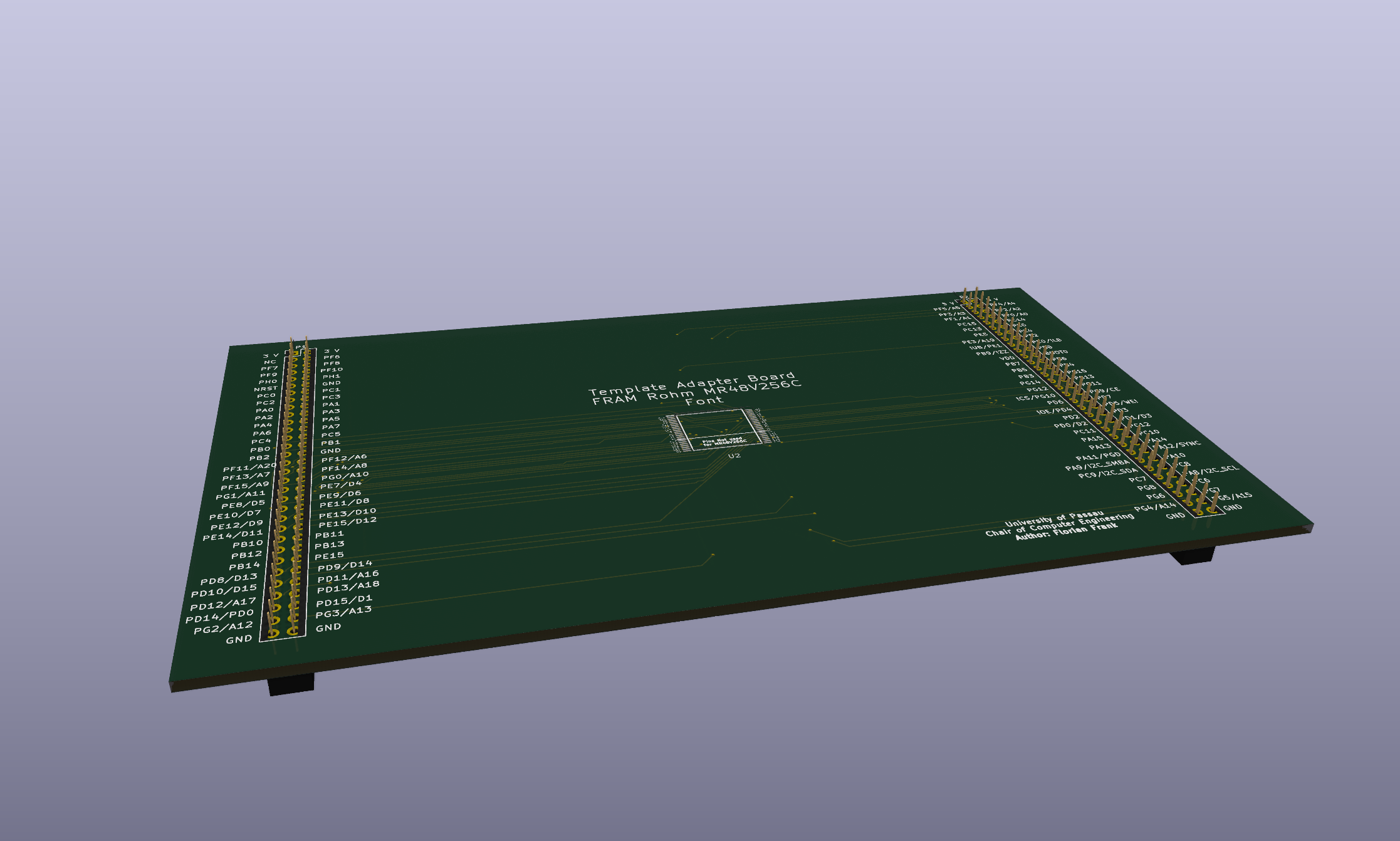
A 3D rendering of the board is shown below:
template_3d_image

Customization for Other Memory Modules

To adapt the design to a different memory device (including alternative packages):

  1. Open the KiCad Project (Adapter_Template_Rohm_FRAM.pro)

The design was created using KiCad 8.0.7.

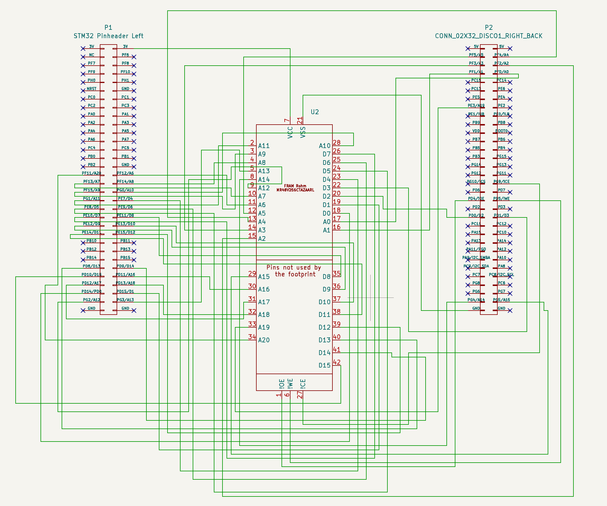
  1. Open the schematic
    • Identify the two 2×32-pin connectors on the left and right:
      • These connect to the FMC adapter board.
      • Do not modify these connectors.
    • Locate the symbol reprenting the memory module in the center:
      • Either modify the symbol to fit your footprint or
      • adjust the footprint to match the existing symbol

The schematic is shown below for reference:
template_3d_image

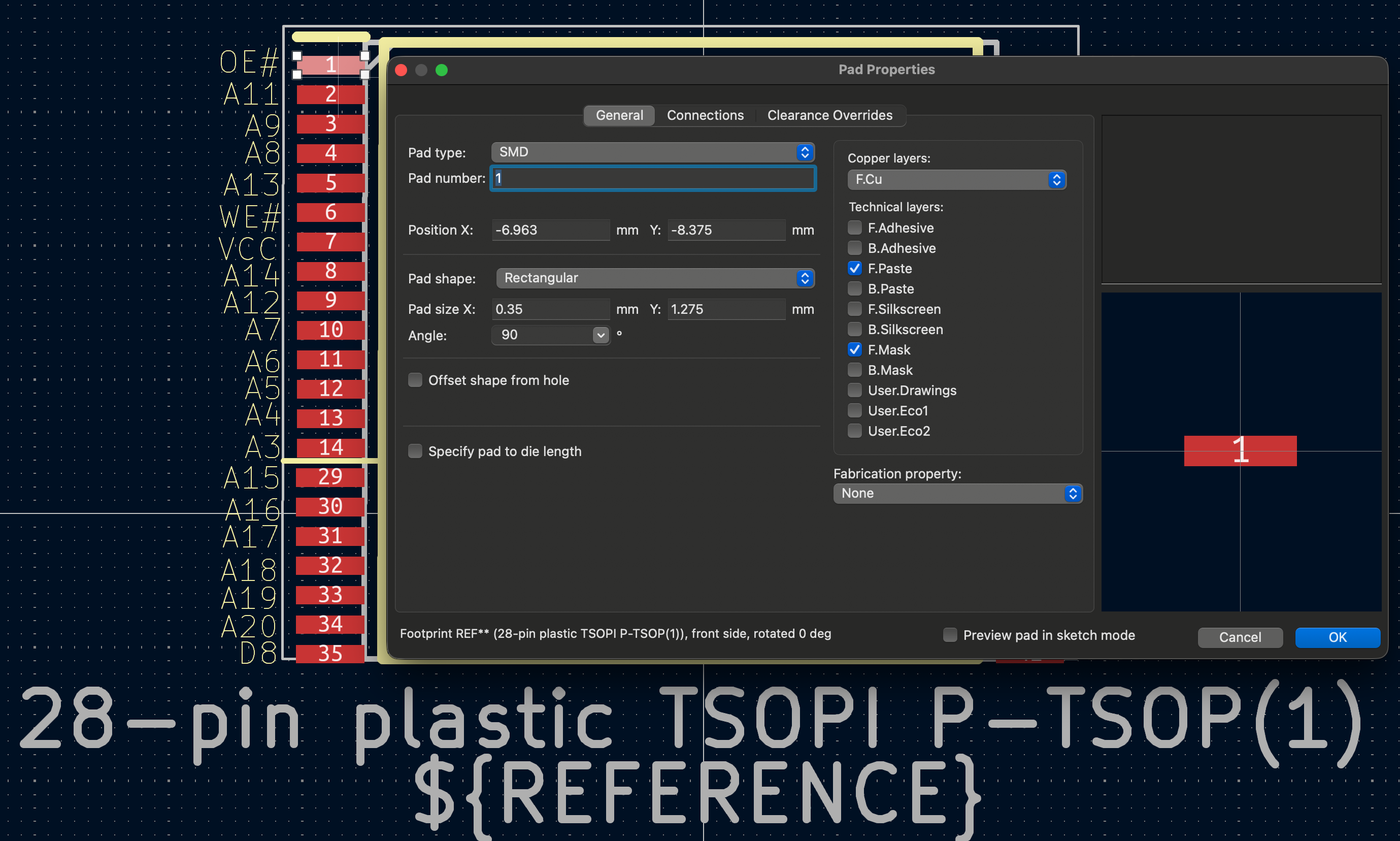
  1. Open the Footprint Editor in KiCad.

To adapt the footprint:

  • Create a new footprint or import an existing one (e.g. from Component Search Engine)
  • Now adjust the pad number so that they match with the ones from the symbol as shown below.
template_3d_image

  1. Assign the footprint to Symbol U2

  2. Export the Netlist `File -> Export -> Netlist``

  3. Open the PCB design (Adapter_Template_Rohm_FRAM.kicad_pcb)

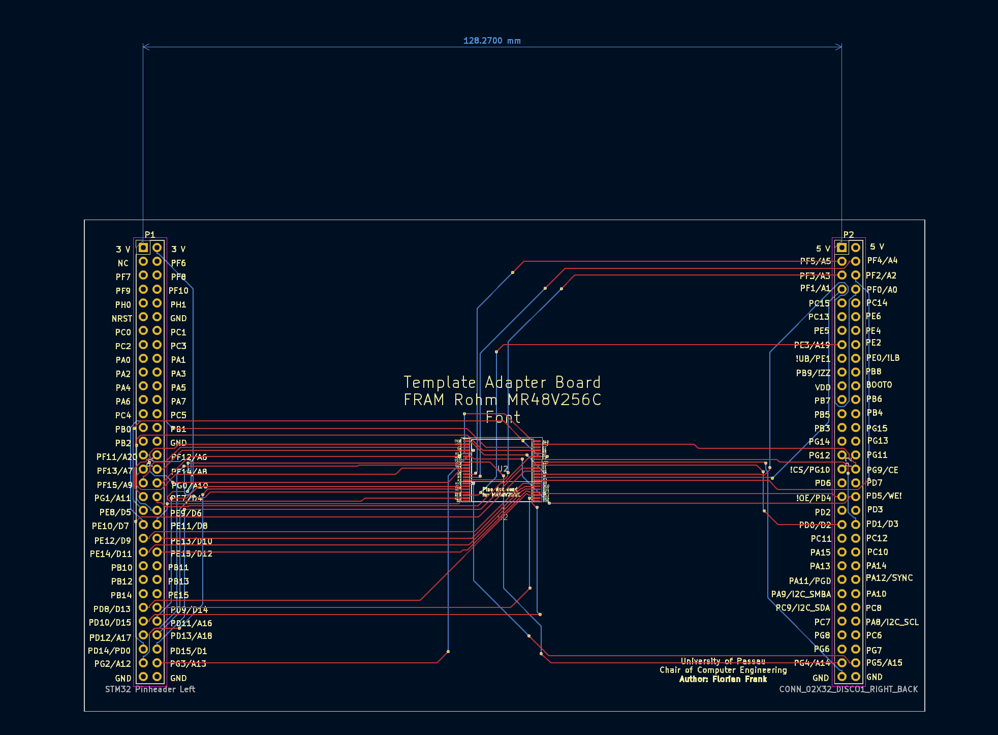
  4. Import the netlist and route the design.

    Rooting may be automized for example by using freerouting

Figure of the reference PCB design:
template_3d_image

  1. Now you can export your Design as Gerber file and produce it as cost efficient two layer PCB.

Parts

36
QtyValueFootprintReferences
12C0805C104K5RAC7411custom_footprints:CAPC2012X88NC1, C2, C3, C4, C5, C6, C7, C8, C9, C10, C11, C12
9MountingHoleMountingHole:MountingHole_2.2mm_M2_Pad_TopBottomH1, H2, H3, H4, H5, H6, H7, H8, H9
6SN74AVC8T245PWG4custom_footprints:SOP65P640X120-24NIC1, IC2, IC3, IC4, IC5, IC6
1ASP-134488-02custom_footprints:ASP13448802J8
1CONN_02X32_DISCO1_LEFT_BACKConnector_PinHeader_2.54mm:PinHeader_2x32_P2.54mm_VerticalP1
1CONN_02X32_DISCO1_RIGHT_BACKConnector_PinHeader_2.54mm:PinHeader_2x32_P2.54mm_VerticalP2
1Conn_01x03Connector_PinHeader_2.54mm:PinHeader_1x03_P2.54mm_VerticalJ9
1Conn_01x04_PinConnector_PinHeader_2.54mm:PinHeader_1x04_P2.54mm_VerticalJ4
1Conn_02x03_Odd_EvenConnector_PinHeader_2.54mm:PinHeader_2x03_P2.54mm_VerticalJ7
1Conn_02x07_Odd_EvenConnector_PinHeader_2.54mm:PinHeader_2x07_P2.54mm_VerticalJ11
1GND_Jumper1Connector_PinHeader_2.54mm:PinHeader_1x02_P2.54mm_VerticalJ1
1PCI-E Extension/Debug Socketcustom_footprints:PCIE_1001878310010TLFJ2

More from FlorianFrank/MemTestX

1
  • 2 layers154.3 × 90.2 mmAdapter Template Rohm FRAM, the printed circuit board in 3D

    Adapter Template Rohm FRAM

    FlorianFrank/MemTestX

    A comprehensive test platform for advanced memory device characterization combining FPGA acceleration, real-time firmware, and automated experiment scheduling

    3 parts1Apache-2.0

Similar boards

  • 4 layers24.4 × 24.4 mmOSO SWAT C1-rounded, the printed circuit board in 3D

    OSO SWAT C1-rounded

    joeycastillo/Sensor-Watch

    A board replacement for the classic Casio F-91W wristwatch

    36 parts2.1k
  • 4 layers19.1 × 19 mmKeyword bottom, the printed circuit board in 3D

    Keyword bottom

    notaroomba/keybytes

    A truly modular keyboard

    36 parts444
  • 4 layers56.4 × 24 mmFilter bank, the printed circuit board in 3D

    Filter bank

    loxodes/vna

    Under development open hardware microwave vector network analyzer

    36 parts205
  • 4 layers74.1 × 24 mmDevelopment board, the printed circuit board in 3D

    Development board

    portapack-mayhem/mayhem-mdk

    PortaPack - Module Develoment Kit

    36 parts88GPL-3.0
  • 4 layers90 × 70 mmDiffpair test, the printed circuit board in 3D

    Diffpair test

    rjwalters/kicad-tools

    Standalone Python tools for parsing and manipulating KiCad schematic and PCB files

    36 parts73MIT
  • 4 layers38 × 38 mmReSDMAC, the printed circuit board in 3D

    ReSDMAC

    mbtaylor1982/ReSDMAC

    Verilog code to replace the Commodore SDMAC found in the A3000

    36 parts51CC-BY-SA-4.0
  • 4 layers30 × 18 mmFdcanusb, the printed circuit board in 3D

    Fdcanusb

    mjbots/fdcanusb

    fdcanusb adapter

    36 parts42Apache-2.0
  • 4 layers45.8 × 49.7 mmRcp rdram, the printed circuit board in 3D

    Rcp rdram

    dmkfasi/nus-cpu

    This tends to re-create Nintendo 64 schematics and lay out a board suitable for portable version

    36 parts35

Questions

How big is the Fmc memory adapter PCB?

It measures 200.1 × 170.2 mm and has 4 copper layers, 1.6 mm thick.

What parts does the Fmc memory adapter use?

36 parts, built around the SN74AVC8T245PWG4 and ASP-134488-02. The full list of its parts is on this page, with links to each part's symbol and footprint where PCBKit's library has them.

Where can I download the Fmc memory adapter KiCad files?

From the FlorianFrank/MemTestX repository on GitHub, at the commit this page was made from: the board is hardware/pcbs/fmc_memory_adapter/fmc_memory_adapter.kicad_pcb and its schematic hardware/pcbs/fmc_memory_adapter/fmc_memory_adapter.kicad_sch. PCBKit opens the board in the browser, with nothing to install.

Can I use the Fmc memory adapter design in my own project?

Its repository publishes it under the Apache-2.0 licence: you may reuse it on that licence's terms (keep the author's notice, and for a copyleft licence share your changes alike).