Skip to the content
2 layers48.3 × 30.5 mmJlink tagConnect adapter v4, the printed circuit board in 3D

Jlink tagConnect adapter v4

Fescron/universal-jlink-adapter101

20 pin SWD/JTAG J-Link to 10 pin (0.1" and 0.05") reconfigurable Cortex-M header with power supply and TagConnect compatibility, as well as with a reset button. (Info about about J-Link Commander and Segger RTT is also given.)

Size
48.3 × 30.5 mm
Copper layers
2
Thickness
1.6 mm
Parts
21
Nets
22
Pads
89
Tracks, vias
139, 12
Pours
1
Routed
Yes
KiCad
KiCad 7 (file 20221018)
Created
19 Sep 2019
Updated
30 Dec 2025

Overview

Jlink tagConnect adapter v4 is an open-source printed circuit board by Fescron, from the Fescron/universal-jlink-adapter repository on GitHub. It is a 2-layer board of 48.3 × 30.5 mm with 21 parts on 22 nets, routed with 139 tracks and 12 vias.

Its parts include 5 connectors, 1 capacitor, 1 resistor and 1 switch. It belongs with the interfaces and adapters and microcontroller boards boards of this library.

README

hardware/jlink-tagConnect-adapter/README.md

jlink-tagConnect-adapter v1.0
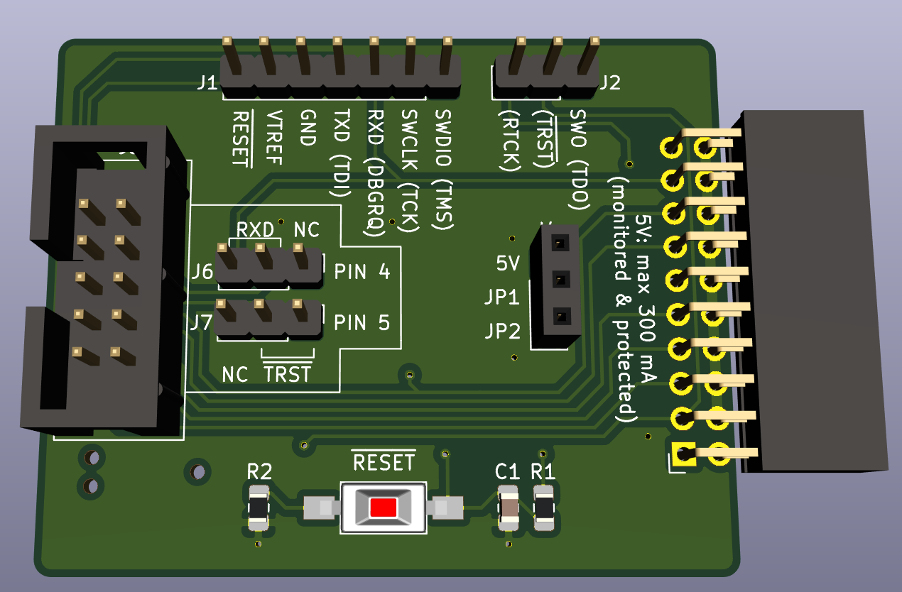
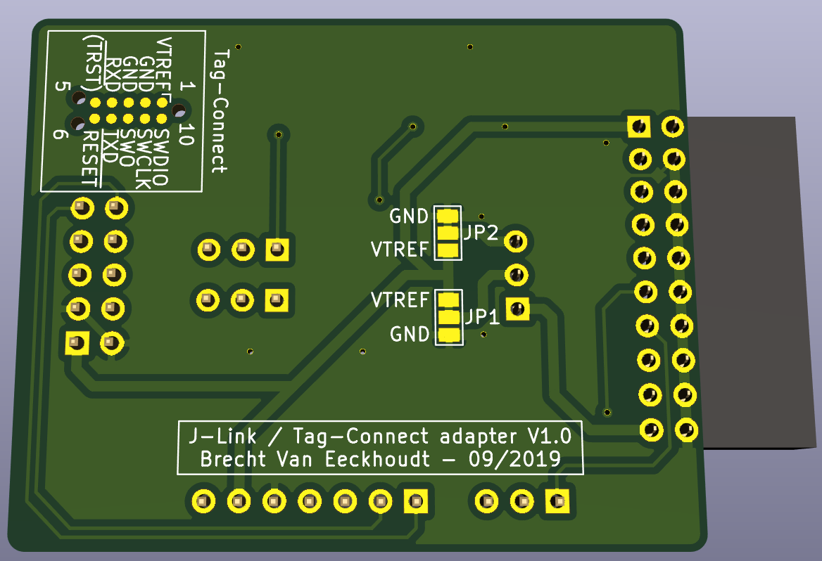
Front Back

This is an old version of the board and was never really used since it didn't follow the J-Link Needle adapter pinout. It's kept here for documentation purposes.


1 - Usage

One can plug this 4cm x 5cm adapter board in a J-Link debugger along with a 10 pin Tag-Connect adapter cable on the IDC connector. The cable will then have the approximate pinout (RXD instead of pin 7 NC) of the standard 9-pin Cortex-M SWD/JTAG pinout from J-Link. The pinout of the Tag-Connect cable can be seen on the picure below (and for reference also on the bottom of the adapter board, but its pins aren't connected).
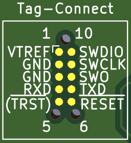
Tag-Connect pinout
  • Pinheaders J1 and J2 can be used to break out the SWD/JTAG pins to a 2.54mm standard header.
  • Pushbutton SW1 can be used to mannually reset the target board.
  • A DC-DC converter can be plugged in on header J4 to supply the target board with the correct voltage using the 5V supply of the J-Link programmer.
    • If the pinout of the converter doesn't match VIN - VOUT - GND, the last two pins can be changed around by swapping the solder joints on JP1 and JP2 on the bottom of the adapter. Then the pinout VIN - GND - VOUT will be selected.
  • Jumpers J6 and J7 can also be used to swap some pinouts around. J6 connects pin 4 on the Tag-Connect cable to RXD or doesn't connect it. J7 connects pin 5 on the Tag-Connect cable to nothing or to nTRST (JTAG).

2 - BOM

ComponentValue
J101x07 Male pinheader
J201x03 Male pinheader
J302x10 Female IDC connector (DigiKey link)
J401x03 Female pinsocket
J502x05 Male IDC header
J601x03 Male pinheader (+ jumper)
J701x03 Male pinheader (+ jumper)
R11 kΩ 0805 Resistor
R2100 Ω 0805 Resistor
C1100 nF 0805 Capacitor
SW12 pin SPST tact switch

Parts

21
QtyValueFootprintReferences
4Jumper_2_BridgedConnector_PinHeader_2.54mm:PinHeader_1x02_P2.54mm_VerticalJP4, JP5, JP8, JP9
3Jumper_3_Bridged12Connector_PinHeader_2.54mm:PinHeader_1x03_P2.54mm_VerticalJP3, JP6, JP7
2SolderJumper_3_Bridged12Jumper:SolderJumper-3_P1.3mm_Bridged12_Pad1.0x1.5mm_NumberLabelsJP1, JP2
1100 nFCapacitor_SMD:C_0603_1608Metric_Pad1.08x0.95mm_HandSolderC1
1100 ΩResistor_SMD:R_0603_1608Metric_Pad0.98x0.95mm_HandSolderR1
1Conn_01x02_PinConnector_PinHeader_2.54mm:PinHeader_1x02_P2.54mm_VerticalJ5
1Conn_01x03Connector_PinSocket_2.54mm:PinSocket_1x03_P2.54mm_VerticalJ4
1Conn_02x05_Odd_EvenConnector_PinHeader_1.27mm:PinHeader_2x05_P1.27mm_VerticalJ3
1Conn_02x05_Odd_EvenConnector_IDC:IDC-Header_2x05_P2.54mm_VerticalJ2
1Conn_02x10_Odd_EvenConnector_PinSocket_2.54mm:PinSocket_2x10_P2.54mm_HorizontalJ1
1SW_PushButton_Switch_THT:SW_PUSH_1P1T_6x3.5mm_H4.3_APEM_MJTP1243SW1
1SolderJumper_2_BridgedJumper:SolderJumper-2_P1.3mm_Bridged_Pad1.0x1.5mmJP10
1Symbol_OSHW-Logo_11.4x12mmBrechtVE_Aesthetics:OSHW-Logo_5.7x6mm_SolderMaskG1

The 19 most common of 21 parts.

More from Fescron/universal-jlink-adapter

3
  • 2 layers48.3 × 30.5 mmJlink tagConnect adapter v3, the printed circuit board in 3D

    Jlink tagConnect adapter v3

    Fescron/universal-jlink-adapter

    20 pin SWD/JTAG J-Link to 10 pin (0.1" and 0.05") reconfigurable Cortex-M header with power supply and TagConnect compatibility, as well as with a reset button.

    15 parts101
  • 2 layers48.3 × 30.5 mmJlink tagConnect adapter v2, the printed circuit board in 3D

    Jlink tagConnect adapter v2

    Fescron/universal-jlink-adapter

    20 pin SWD/JTAG J-Link to 10 pin (0.1" and 0.05") reconfigurable Cortex-M header with power supply and TagConnect compatibility, as well as with a reset button.

    14 parts101
  • 2 layers50 × 40.1 mmJlink tagConnect adapter, the printed circuit board in 3D

    Jlink tagConnect adapter

    Fescron/universal-jlink-adapter

    20 pin SWD/JTAG J-Link to 10 pin (0.1" and 0.05") reconfigurable Cortex-M header with power supply and TagConnect compatibility, as well as with a reset button.

    14 parts101

Similar boards

  • 2 layers28.3 × 39.8 mmLevelShifter, the printed circuit board in 3D

    LevelShifter

    gusmanb/logicanalyzer

    24 channel, 100Msps logic analyzer hardware and software

    21 parts5.1kGPL-3.0
  • 2 layers171.2 × 72.9 mmAmiga gfxcard before pour, the printed circuit board in 3D

    Amiga gfxcard before pour

    mntmn/amiga2000-gfxcard

    MNT VA2000, an Open Source Amiga 2/3/4000 Graphics Card (Zorro II/III), written in Verilog

    21 parts1k
  • 2 layers93.9 × 46 mmRectifier, the printed circuit board in 3D

    Rectifier

    rene-dev/stmbl

    AC Servo Driver for STM32F4

    21 parts990GPL-3.0
  • 2 layers45.5 × 42.9 mmEsphome han reader, the printed circuit board in 3D

    Esphome han reader

    hackclub/OnBoard

    💡 Join 1,000 teenagers and make your first PCB with a $100 grant!

    21 parts915
  • 2 layers31.8 × 14.5 mmEsp prog, the printed circuit board in 3D

    Esp prog

    drandyhaas/KiCadRoutingTools

    A set of Python/Rust tools to aid routing in KiCad

    21 parts744MIT
  • 2 layers23.5 × 15.8 mmQuiverAttachPCB, the printed circuit board in 3D

    QuiverAttachPCB

    Arrow-air/project-quiver

    Project Quiver documentation, designs, and project artifacts.

    21 parts617CERN-OHL-S-2.0
  • 2 layers69.9 × 41.3 mmHeaterMeterLCD, the printed circuit board in 3D

    HeaterMeterLCD

    CapnBry/HeaterMeter

    HeaterMeter and LinkMeter Arduino BBQ Controller

    21 parts557MIT
  • 2 layers161.3 × 111.8 mmDoj, the printed circuit board in 3D

    Doj

    kelu124/echomods

    Open source ultrasound processing modules and building blocks

    21 parts463

Questions

How big is the Jlink tagConnect adapter v4 PCB?

It measures 48.3 × 30.5 mm and has 2 copper layers, 1.6 mm thick.

What parts does the Jlink tagConnect adapter v4 use?

21 parts. The full list of its parts is on this page, with links to each part's symbol and footprint where PCBKit's library has them.

Where can I download the Jlink tagConnect adapter v4 KiCad files?

From the Fescron/universal-jlink-adapter repository on GitHub, at the commit this page was made from: the board is hardware/jlink-tagConnect-adapter-v4/jlink-tagConnect-adapter-v4.kicad_pcb and its schematic hardware/jlink-tagConnect-adapter-v4/jlink-tagConnect-adapter-v4.kicad_sch. PCBKit opens the board in the browser, with nothing to install.

Can I use the Jlink tagConnect adapter v4 design in my own project?

Its repository states no licence, so its author keeps all rights: ask Fescron before reusing the design.