

2 layers115.6 × 106.7 mm
ErgoSNM v3 left
siderakb/ergo-snm-keyboard
ErgoSNM is a split ergonomic keyboard integrated with trackball, wireless is in beta
90 parts172CERN-OHL-P-2.0

自制WCH-LinkE
LinkE is an open-source printed circuit board by ErBWs, from the ErBWs/WCH-LinkE-Nano repository on GitHub, published under the GPL-3.0 licence. It is a 2-layer board of 26.4 × 13.7 mm with 25 parts on 30 nets, routed with 213 tracks and 32 vias.
It is built around the RT9013-33GB. Its parts include 7 resistors, 6 capacitors, 4 diodes, 2 ICs and 2 switches. It belongs with the RISC-V boards of this library.
自制WCH-LinkE
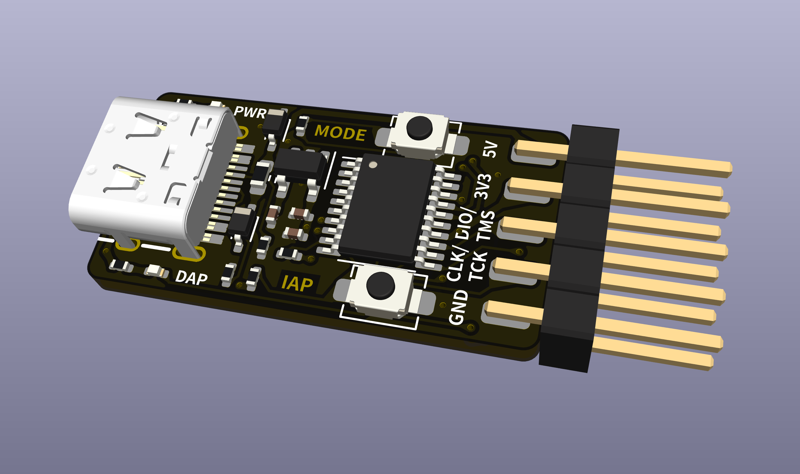
准备好一个WCH-Link,可以考虑我之前制作的这款。
这个下载器需要另一个wch-link才可以自制,很麻烦所以我一开始没考虑,但是下载速度的确很快
直接打开3.Software文件夹内的WCH-LinkUtility.exe
载入2.Firmware内的.bin文件并烧录
断电重新上电即可作为正常WCH-LinkE使用
持续按住MODE键上电,等待一段时间后松开可在Link-RV和DAP模式中切换
| Qty | Value | Footprint | References |
|---|---|---|---|
| 3 | 10K | ErBW_s:R_0402 | R3, R4, R6 |
| 2 | 100nF | ErBW_s:C_0402 | C1, C8 |
| 2 | 22pF | ErBW_s:C_0402 | C4, C5 |
| 2 | 4.7K | ErBW_s:R_0402 | R1, R2 |
| 1 | 0R | ErBW_s:R_0402 | R7 |
| 1 | 10nF | ErBW_s:C_0402 | C3 |
| 1 | 10uF | ErBW_s:C_0402 | C2 |
| 1 | 12MHz | ErBW_s:Crystal_SMD_3225_4P | Y1 |
| 1 | 1K | ErBW_s:R_0402 | R5 |
| 1 | 1N5819 | ErBW_s:SOD-323 | D3 |
| 1 | 500mA | Fuse:Fuse_0603_1608Metric | F1 |
| 1 | BLUE | ErBW_s:LED_0402 | D4 |
| 1 | CH32V305FBT6 | Package_SO:TSSOP-20_4.4x6.5mm_P0.65mm | U2 |
| 1 | Conn_02x05_Odd_Even | ErBW_s:Debug_Header_2x05 | J2 |
| 1 | ESD | ErBW_s:SOD-323 | D2 |
| 1 | GREEN | ErBW_s:LED_0402 | D1 |
| 1 | IAP | ErBW_s:BUTTON_3x4 | SW2 |
| 1 | ModeS | ErBW_s:BUTTON_3x4 | SW1 |
| 1 | RT9013-33GB | Package_TO_SOT_SMD:SOT-23-5 | U1 |
| 1 | USB-Type-C | ErBW_s:USB-Type-C_SMD_16P | J? |
siderakb/ergo-snm-keyboard
ErgoSNM is a split ergonomic keyboard integrated with trackball, wireless is in beta


phonght32/OpenDrone_HW_AIO_FC_F405
OpenDrone Project - AIO Brushless FC F405.


martinberlin/bistable-smart-switch
An epaper switch project with 2 PCBs, controller+touch, and 220AC to 3DC with Relay (Latch or solid-state)

It measures 26.4 × 13.7 mm and has 2 copper layers, 1.6 mm thick.
25 parts, built around the RT9013-33GB. The full list of its parts is on this page, with links to each part's symbol and footprint where PCBKit's library has them.
From the ErBWs/WCH-LinkE-Nano repository on GitHub, at the commit this page was made from: the board is 1.Hardware/LinkE.kicad_pcb and its schematic 1.Hardware/LinkE.kicad_sch. PCBKit opens the board in the browser, with nothing to install.
Its repository publishes it under the GPL-3.0 licence: you may reuse it on that licence's terms (keep the author's notice, and for a copyleft licence share your changes alike).