2 layers
Encoder
byrantech/laptop
anyon_e, a highly integrated, high end, open source laptop. Attempt the impossible.
7 parts4.3kMIT

 DevonHope/HMD-Fusion-DIY-Cases4
A repo for storing my progress in developing a case/outift for the HMD Fusion phone
Breakout Flex PCB Testing Stand is an open-source printed circuit board by DevonHope, from the DevonHope/HMD-Fusion-DIY-Cases repository on GitHub, published under the MIT licence. It is a 2-layer board of 145 × 27 mm with 7 parts on 6 nets, routed with 52 tracks and 0 vias.
It belongs with the interfaces and adapters boards of this library.
A repo for storing my progress into developing a case/outift for the HMD Fusion phone. This repo includes schematic drawings, PCB drawings, and 3D models for the breakout board and testbench case. This repo will also include future dev kits for cases/outfits that make use of the exposed pins on the back of the HMD Fusion.
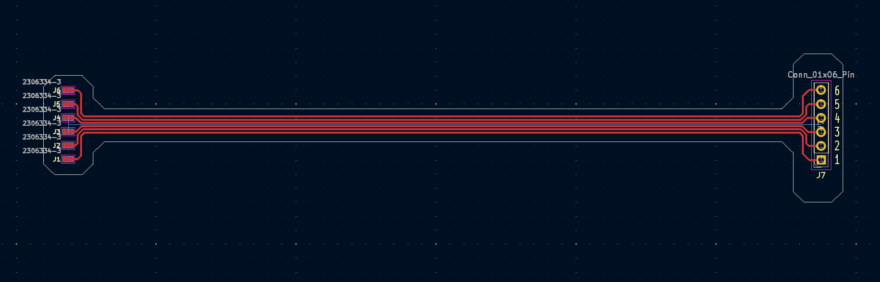 KiCAD V8 PCB drawing
The breakout board is used to breakout the 6 pin header on the back of the phone and expand it into the ISO standard 2.54mm/0.1" 6 pin header for breadboard testing and development of external circuits. This board should be manufactured using a flexible PCB material, the case and basic funcationality of the spring pins were designed with this in mind.
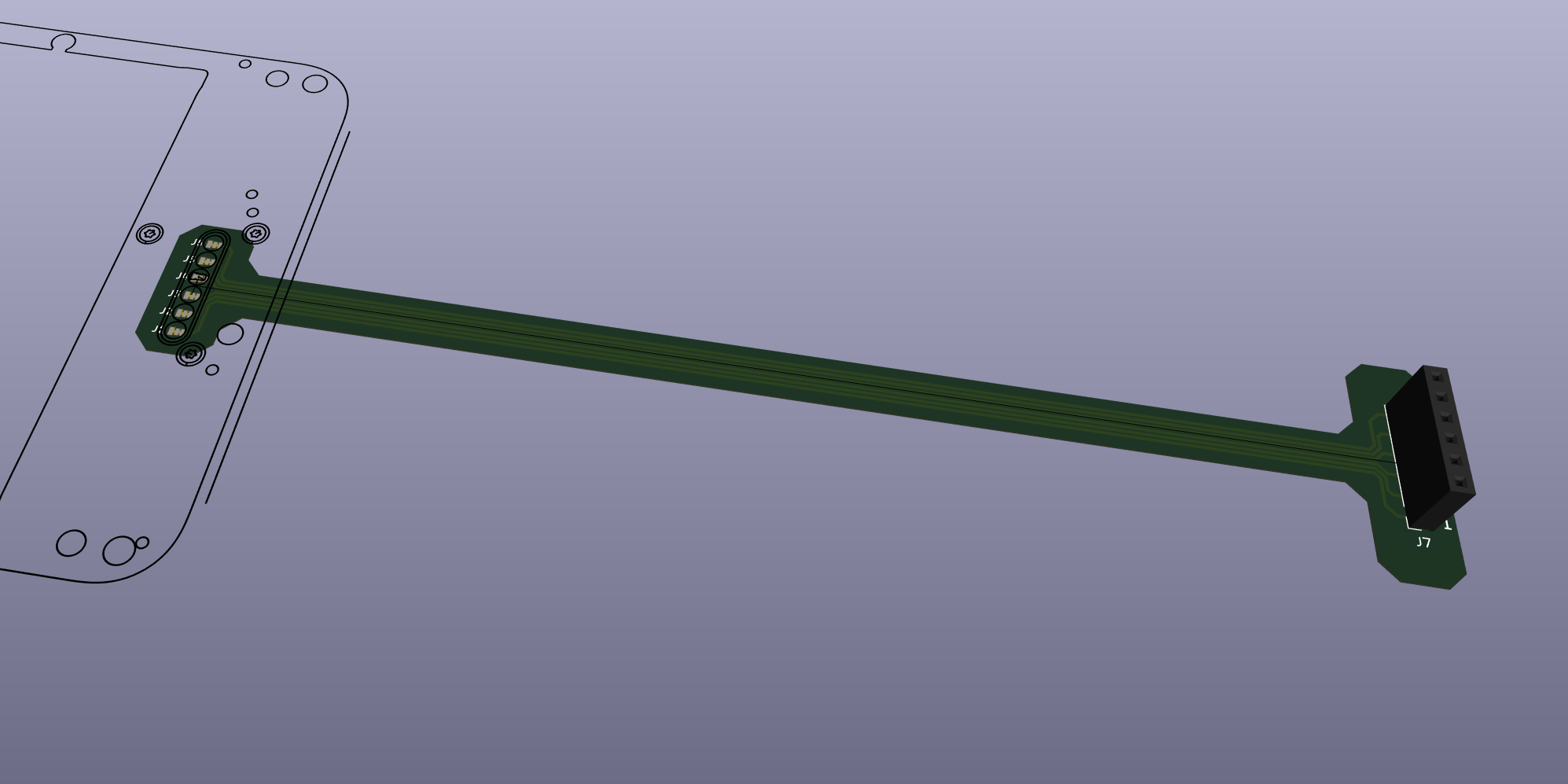 KiCAD V8 3D Model Drawing
There is a testbench case to go with this, it is best printed in TPU or other flexible materials to ensure the spring loaded pins on the breakout board do not get bent or damaged when removing the phone from the case. To insert the PCB into the case there are three edges that overlap the cutout of the PCB slot, this is a simple method used for the time being to get simple testing done but will be modified for an actual test run of a case/outfit.
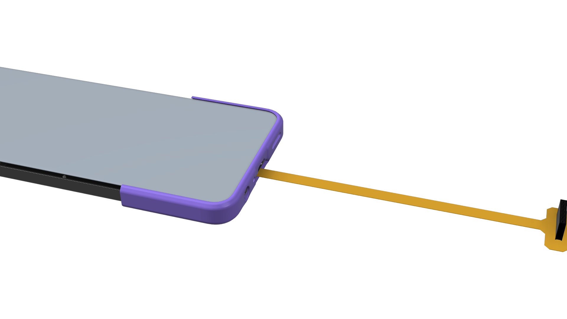 Testbench Case Bottom Half V1R1
| Qty | Value | Footprint | References |
|---|---|---|---|
| 6 | 2306334-3 | custom symbols:TE_2306334-3 | J1, J2, J3, J4, J5, J6 |
| 1 | Conn_01x06_Pin | Connector_PinSocket_2.54mm:PinSocket_1x06_P2.54mm_Vertical | J7 |
byrantech/laptop
anyon_e, a highly integrated, high end, open source laptop. Attempt the impossible.


AxxAxx/AxxSolder
STM32 Based soldering station for JBC cartridges, 9-24 VDC and USB-PD power


jamro/tiny-engineer
A small desktop robot that brings an AI coding assistant to life, physically acting out when it reads files, thinks, writes code, and finishes work.

hoglet67/RGBtoHDMI
Bare-metal Raspberry Pi project that provides pixel-perfect sampling of Retro Computer RGB/YUV video and conversion to HDMI

It measures 145 × 27 mm and has 2 copper layers, 0.2 mm thick.
7 parts. The full list of its parts is on this page, with links to each part's symbol and footprint where PCBKit's library has them.
From the DevonHope/HMD-Fusion-DIY-Cases repository on GitHub, at the commit this page was made from: the board is Development/Breakout-Flex-PCB-Testing-Stand/Breakout-Flex-PCB-Testing-Stand.kicad_pcb and its schematic Development/Breakout-Flex-PCB-Testing-Stand/Breakout-Flex-PCB-Testing-Stand.kicad_sch. PCBKit opens the board in the browser, with nothing to install.
Its repository publishes it under the MIT licence: you may reuse it on that licence's terms (keep the author's notice, and for a copyleft licence share your changes alike).