2 layers98 × 27 mm

 Deepu-Bhai5/two-led-indicator-pcb1
A beginner KiCad PCB design project for a two-channel LED indicator, covering schematic capture, PCB layout, routing, DRC validation, and Gerber generation.
Two led indicator is an open-source printed circuit board by Deepu-Bhai5, from the Deepu-Bhai5/two-led-indicator-pcb repository on GitHub. It is a 2-layer board of 35.5 × 20.8 mm with 5 parts on 5 nets, routed with 30 tracks and 0 vias.
Its parts include 2 resistors, 2 diodes and 1 connector.
A beginner PCB design project developed in KiCad as an introduction to the complete PCB design workflow, from schematic capture to manufacturing file generation.
This project is a simple two-channel LED indicator PCB.
Each LED is independently controlled through its own current-limiting resistor, with a common ground connection.
The board uses:
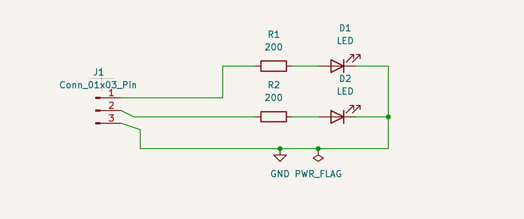
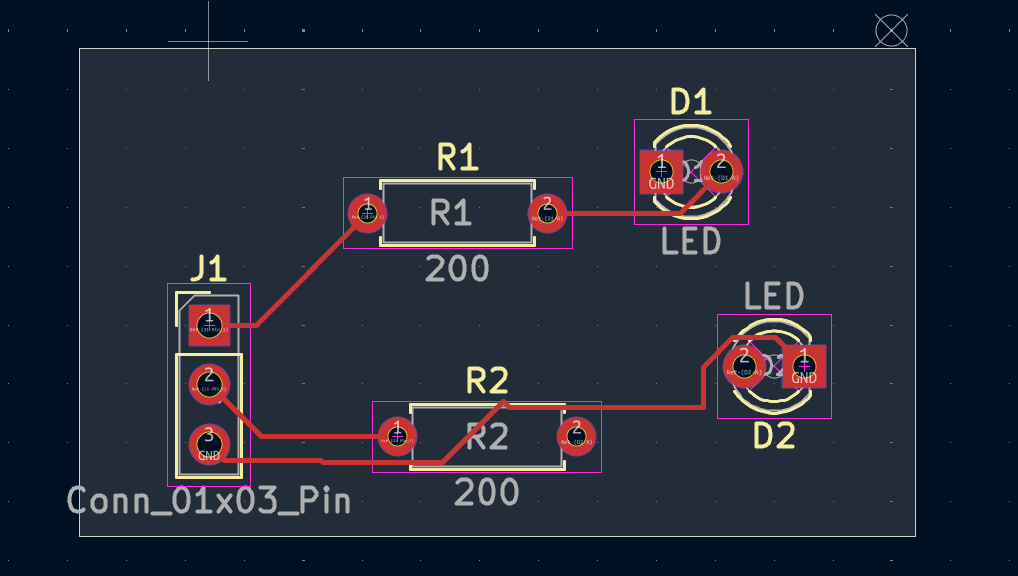
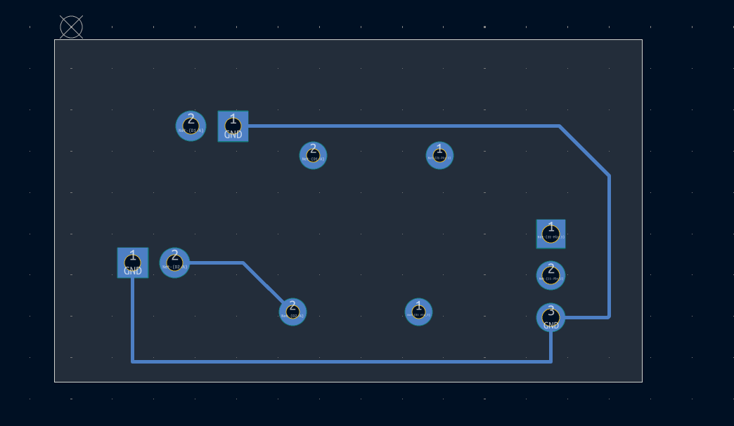
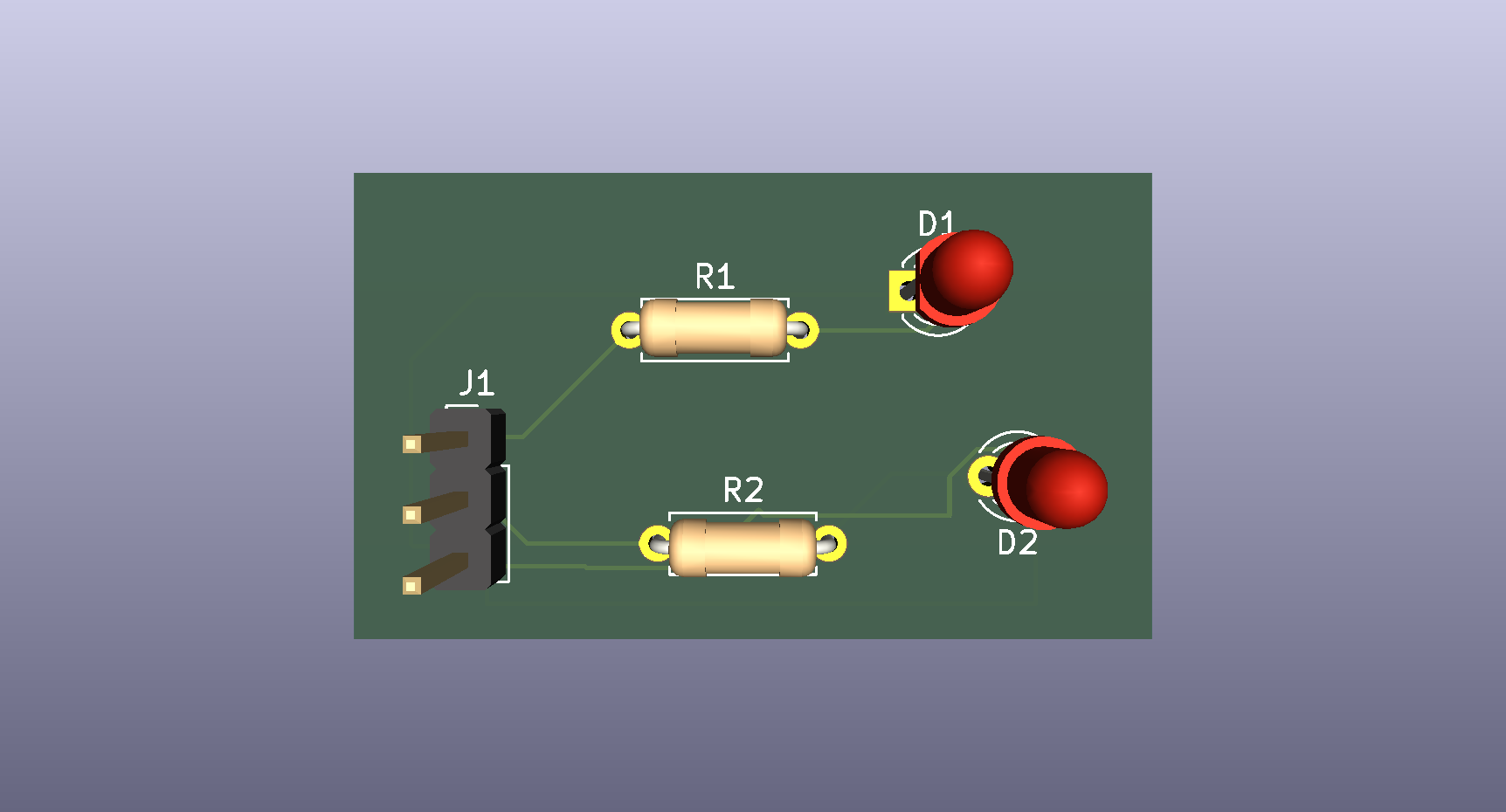
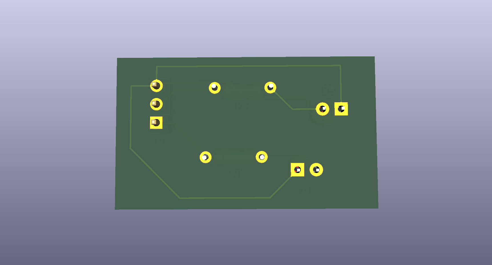
The PCB was checked using KiCad's Design Rule Checker.
Validation included:
Gerber and drill files were generated using KiCad's manufacturing output tools.
The final PCB design was evaluated using external Design for Manufacturing (DFM) tools. The design passed checks covering:
The design is currently ready for PCB fabrication. Physical fabrication, assembly, and electrical testing are pending.
During development, several issues were identified and corrected, including:
These issues were resolved through iterative PCB inspection and validation.
Design: Complete
Electrical validation: Complete
KiCad DRC: Passed
Manufacturing DFM: Passed
Gerber files: Generated
Fabrication status: Ready for manufacturing
Physical testing: Pending
| Parameter | Value |
|---|---|
| PCB Layers | 2 |
| Board Size | ~35.5 × 20.75 mm |
| Components | Through-hole |
| Resistors | 200 Ω × 2 |
| LEDs | 3 mm × 2 |
| Input Connector | 1×3, 2.54 mm |
| Board Thickness | 1.6 mm |
| Copper | 1 oz |
Deep Das
B.Tech ECE Student at Delhi Technological University (DTU)
| Qty | Value | Footprint | References |
|---|---|---|---|
| 2 | 200 | Resistor_THT:R_Axial_DIN0207_L6.3mm_D2.5mm_P7.62mm_Horizontal | R1, R2 |
| 2 | LED | LED_THT:LED_D3.0mm | D1, D2 |
| 1 | Conn_01x03_Pin | Connector_PinHeader_2.54mm:PinHeader_1x03_P2.54mm_Vertical | J1 |

joypad-ai/joypad-os
Universal controller firmware for building adapters, dongles, and custom controllers.

OLIMEX/OLINUXINO
OLINUXINO is Open Source / Open Hardware, low cost from EUR 24 Linux Industrial grade Single Board Computer capable to operate -25+85C

jamro/tiny-engineer
A small desktop robot that brings an AI coding assistant to life, physically acting out when it reads files, thinks, writes code, and finishes work.

hackclub/OnBoard
💡 Join 1,000 teenagers and make your first PCB with a $100 grant!


Luos-io/luos_engine
Open-source and real-time orchestrator for cyber-physical-systems, to easily design, test and deploy embedded applications and digital twins.
It measures 35.5 × 20.8 mm and has 2 copper layers, 1.6 mm thick.
5 parts. The full list of its parts is on this page, with links to each part's symbol and footprint where PCBKit's library has them.
From the Deepu-Bhai5/two-led-indicator-pcb repository on GitHub, at the commit this page was made from: the board is Kicad/KiCad/two-led-indicator.kicad_pcb and its schematic Kicad/KiCad/two-led-indicator.kicad_sch. PCBKit opens the board in the browser, with nothing to install.
Its repository states no licence, so its author keeps all rights: ask Deepu-Bhai5 before reusing the design.