2 layers159.5 × 30 mm
Type f
google/mozc-devices
Circuit diagrams and firmware source code for Gboard DIY keyboards
25 parts3kApache-2.0

 DagaVedant/NotGoingToBeLateToSchool
a 9-key bedside alarm clock thats also a ambient info display, wakes you up by telling your phone to play Spotify, and only lets you snooze three times before you have to type a code to shut it up.
Kicad schematic is an open-source printed circuit board by DagaVedant, from the DagaVedant/NotGoingToBeLateToSchool repository on GitHub, published under the MIT licence. It is a 2-layer board of 69.5 × 97 mm with 25 parts on 24 nets, routed with 461 tracks and 14 vias.
Its parts include 9 diodes, 9 switches, 1 IC and 1 connector. It belongs with the lEDs and displays boards and the ESP32 and RISC-V boards of this library.
a 9 key alarm clock that makes you type a code to shut it up.
built on a xiao esp32c3 for BLARE. during the day it sits on my desk cycling through weather, hackatime hours, now playing and world clocks. at 6am it tells my phone to start playing spotify instead of screaming at me with a piezo. you get 3 snoozes, and on the 3rd one you have to type a code on the keypad before it stops.
every alarm clock i've had is useless for the 16 hours a day you're awake, and way too easy to snooze into oblivion. this one tries to fix both.
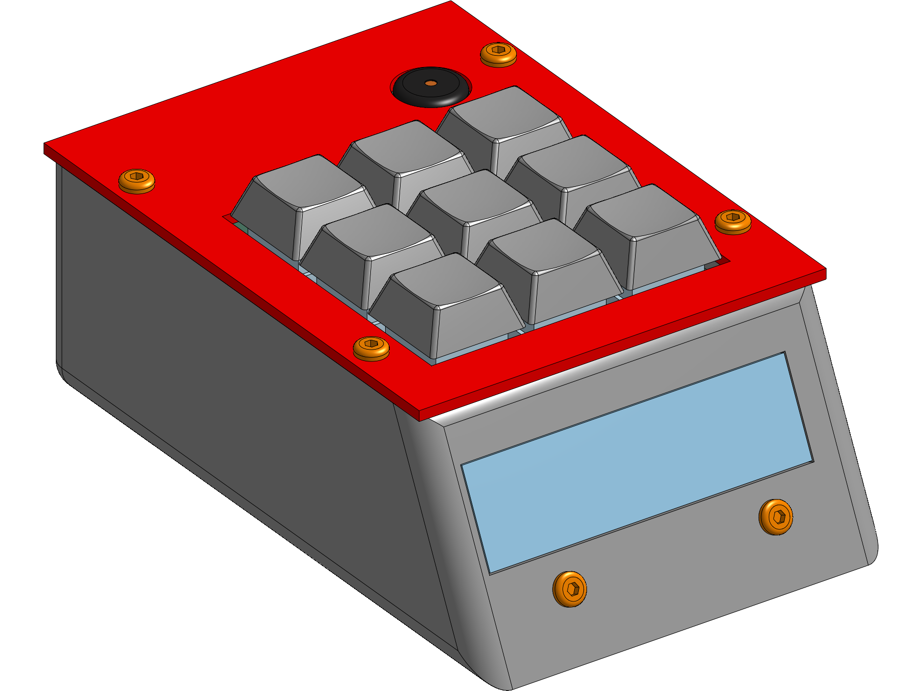
the top plate and the pcb share hardware: one m3x16 screw per corner runs down through the top plate boss and the board into the same heatset insert the pcb post already carries, so there's no separate top-plate insert or screw anymore. simpler, but the board can't come out without pulling the top plate first. the bosses sit over the board, so they need a bit of support when printing the base.
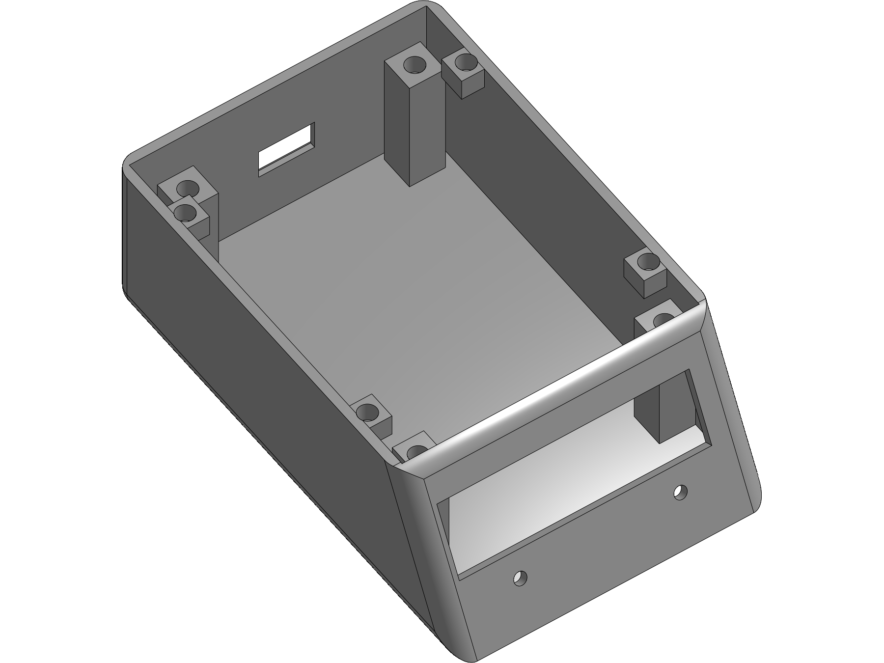
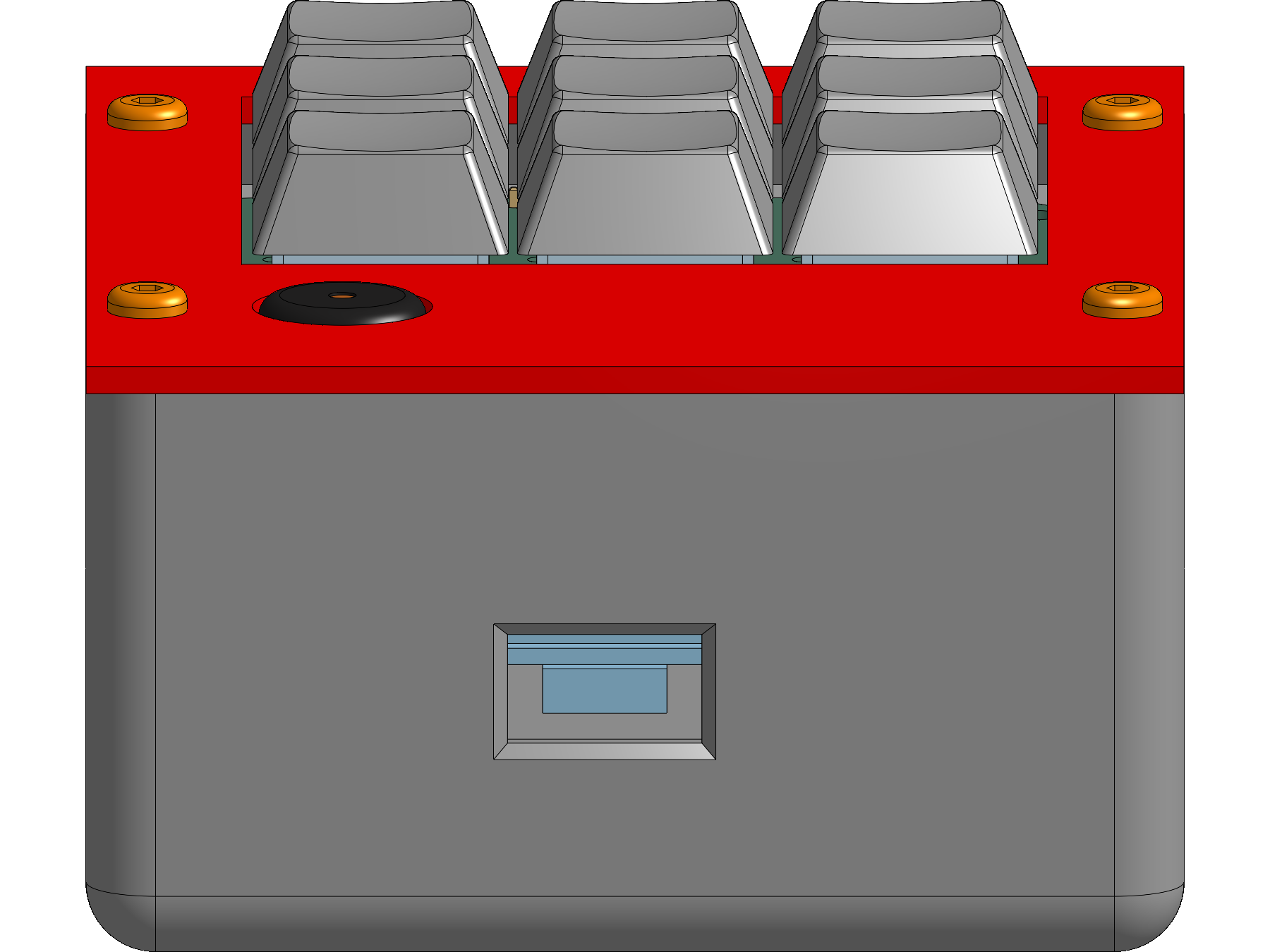
the pcb sits on four posts that land exactly on its mounting holes. the xiao is socketed on the underside, so its usb-c port ends up 13mm below the board, and the slot in the back wall is cut around that spot, not at board height.
ambient, all day
alarm, at 6am
ble, written and compiling, never run on hardware
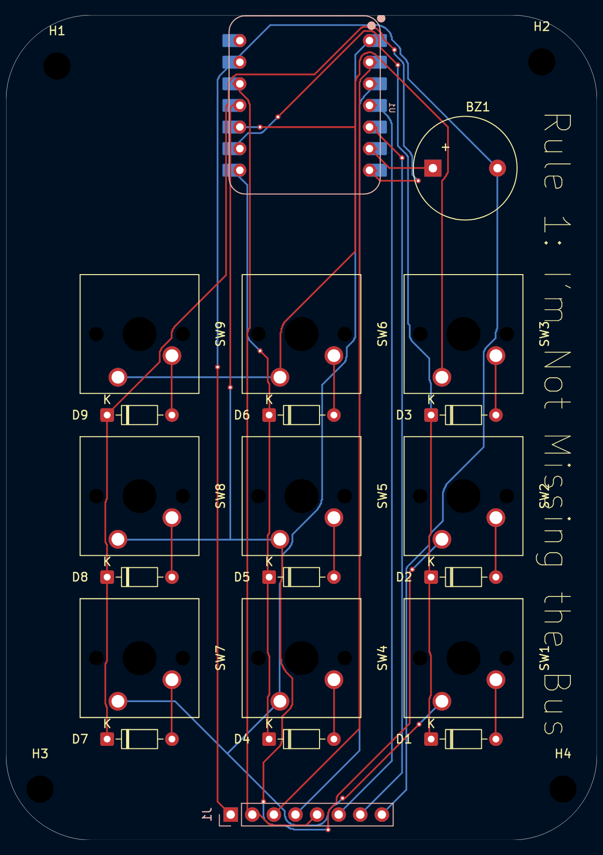
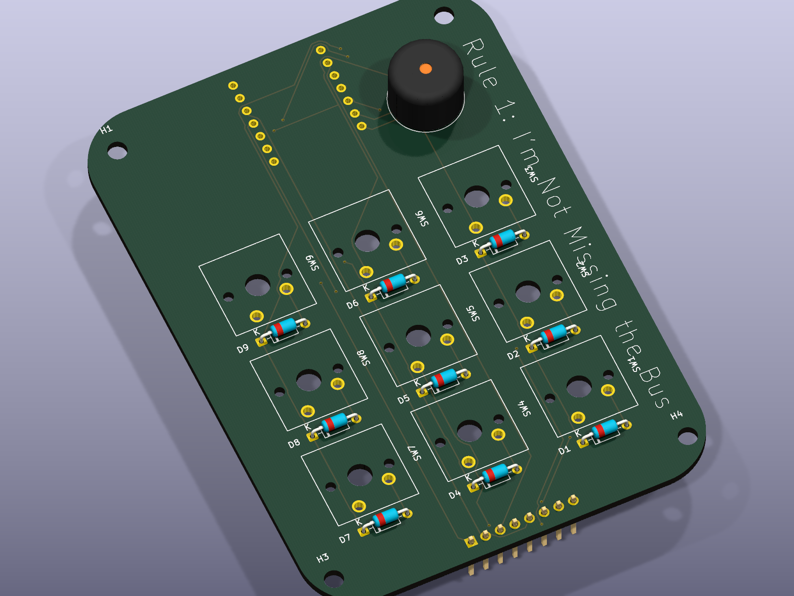
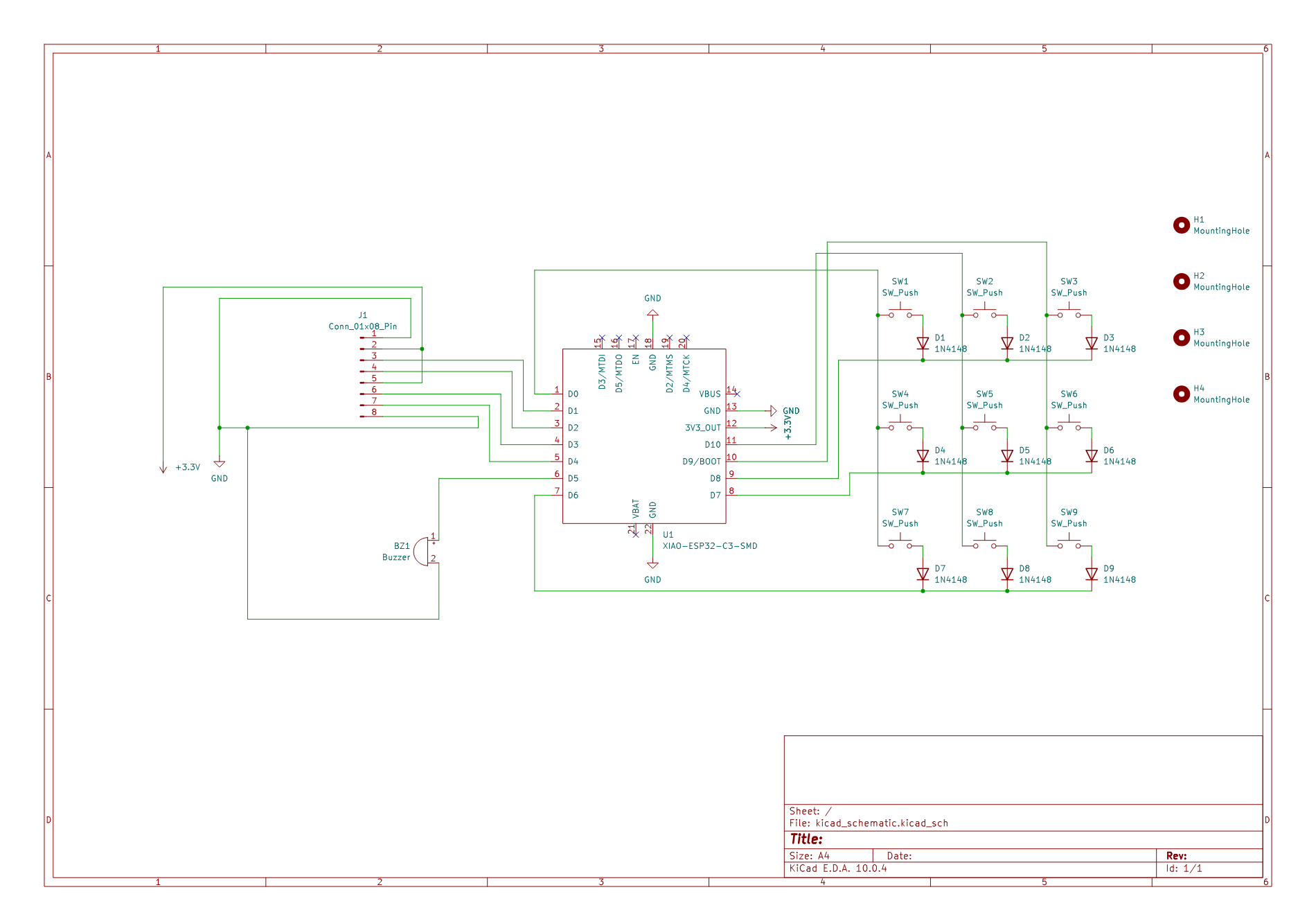
69.5 x 97mm, 2 layers, 25 footprints. 461 tracks, 14 vias, about 1.5m of copper. drc clean, nothing unrouted.
the routed layout in kicad, red is the front copper and blue is the back:
and a 3d render of the same board:
nine switches in a 3x3 matrix, one 1n4148 per key so holding two keys down cannot ghost a third.
| part | qty |
|---|---|
| seeed xiao esp32c3 | 1 |
| st7789 tft (76×284) | 1 |
| cherry mx pcb-mount switches | 9 |
| mx keycaps | 9 |
| 1n4148 diodes | 9 |
| piezo buzzer (12×9.5, rm7.6) | 1 |
| 1×08 2.54mm pin socket (display) | 1 |
| 1×07 2.54mm pin sockets (xiao) | 2 |
| m3×16 screws | 4 |
| m3 heatset inserts | 4 |
same list in BOM.csv.
| Qty | Value | Footprint | References |
|---|---|---|---|
| 9 | 1N4148 | Diode_THT:D_DO-35_SOD27_P7.62mm_Horizontal | D1, D2, D3, D4, D5, D6, D7, D8, D9 |
| 9 | SW_Push | Button_Switch_Keyboard:SW_Cherry_MX_1.00u_PCB | SW1, SW2, SW3, SW4, SW5, SW6, SW7, SW8, SW9 |
| 4 | MountingHole | MountingHole:MountingHole_3.2mm_M3 | H1, H2, H3, H4 |
| 1 | Buzzer | Buzzer_Beeper:Buzzer_12x9.5RM7.6 | BZ1 |
| 1 | Conn_01x08_Pin | Connector_PinSocket_2.54mm:PinSocket_1x08_P2.54mm_Vertical | J1 |
| 1 | XIAO-ESP32-C3-SMD | Seeed_XIAO:XIAO-ESP32-C3-DIP | U1 |
google/mozc-devices
Circuit diagrams and firmware source code for Gboard DIY keyboards

davidphilipbarr/Sweep
Sweep - a small promicro based keyboard inspired by the Ferris.


hackclub/OnBoard
💡 Join 1,000 teenagers and make your first PCB with a $100 grant!

xyphro/UsbGpib
Versatile, cheap and portable USB to GPIB converter (USBTMC class based)


jes/scamp-cpu
A homebrew 16-bit CPU with a homebrew Unix-like-ish operating system.

It measures 69.5 × 97 mm and has 2 copper layers, 1.6 mm thick.
25 parts. The full list of its parts is on this page, with links to each part's symbol and footprint where PCBKit's library has them.
From the DagaVedant/NotGoingToBeLateToSchool repository on GitHub, at the commit this page was made from: the board is PCB/kicad_schematic/kicad_schematic.kicad_pcb and its schematic PCB/kicad_schematic/kicad_schematic.kicad_sch. PCBKit opens the board in the browser, with nothing to install.
Its repository publishes it under the MIT licence: you may reuse it on that licence's terms (keep the author's notice, and for a copyleft licence share your changes alike).