8 layers35.5 × 25 mm

 CopperPilot/rpi-zero-2w-kicad1
KiCad port of jonny12375/rp3a0: Raspberry Pi Zero 2W's RP3A0 on a Pi Pico-sized board
Rp3a0-mini is an open-source printed circuit board by CopperPilot, from the CopperPilot/rpi-zero-2w-kicad repository on GitHub. It is a 6-layer board of 60 × 20.4 mm with 124 parts on 232 nets, routed with 2,045 tracks and 397 vias.
It is built around the PAM2306AYPKE, RT8088AWSC and EXC24CH900U, with the 0402CG300J500NT, CL21A476MQYNNNE and 0402CG101J500NT among its other parts. Its parts include 47 capacitors, 25 resistors, 6 inductors, 5 ICs and 5 connectors.


This directory contains the native KiCad 10 schematic, 6-layer PCB layout, project-local symbol/footprint libraries, PyTest verification suite, and automated JLCPCB fabrication/assembly export pipeline for the RP3A0 Pico.
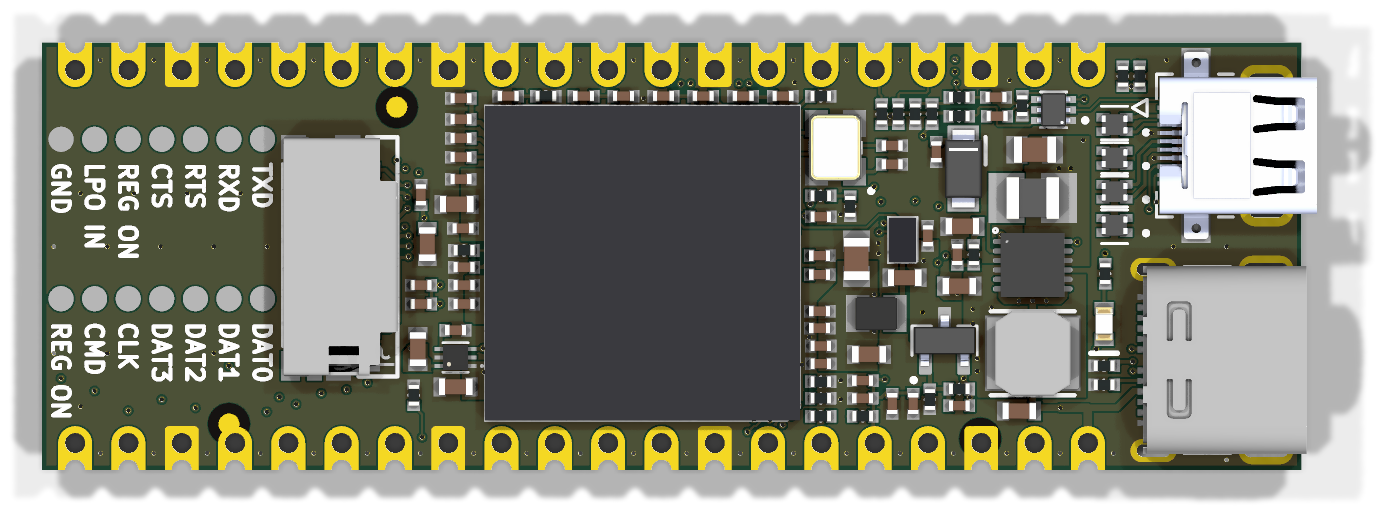
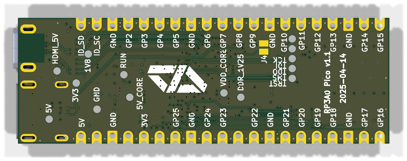
60.00 mm × 20.35 mm (51.00 mm × 20.35 mm standard Raspberry Pi Pico castellated body + 9.00 mm right-hand overhang for Micro-HDMI J2 and USB-C J3).F.Cu, In1.Cu, In2.Cu, In3.Cu, In4.Cu, B.Cu), 1.61 mm nominal thickness, ENIG (Electroless Nickel Immersion Gold) surface finish required for 0.65 mm BGA (U1) and 0.40 mm WLCSP (U3) coplanarity.FID1 at (127.4, 113.0), FID2 at (135.4, 97.9), FID3 at (163.2, 113.7)) with 1.0 mm copper circles, 2.0 mm solder mask openings, and 2.1 mm copper-pour keepouts.0.95 mm drill) on J5 along top (y = 94.8286 mm) and bottom (y = 115.1786 mm) board edges.| Rule Parameter | Design Minimum | JLCPCB 6-Layer Capability | Status |
|---|---|---|---|
| Minimum Track Width | 0.0889 mm (3.5 mil) | 0.0889 mm (3.5 mil) | Compliant |
| Minimum Copper Clearance | 0.0889 mm (3.5 mil) | 0.0889 mm (3.5 mil) | Compliant |
| Minimum Via Drill / Pad | 0.20 mm / 0.35 mm (0.30 mm rule) | 0.20 mm / 0.30 mm | Compliant |
| Minimum Annular Ring | 0.075 mm (0.05 mm rule) | 0.05 mm | Compliant |
Fine-Pitch Solder Mask Web (U3, J2) | 0.15 mm (U3), 0.202 mm (J2) | 0.10 mm (Green LPI) | Compliant |
| Minimum Silkscreen Text Height | 0.80 mm (0.15 mm stroke) | 0.80 mm (0.15 mm stroke) | Compliant |
In1.Cu (0.100 mm below F.Cu), In4.Cu (0.100 mm above B.Cu), and B.Cu carry stitched GND copper pours tied together by 107 through-hole GND stitching vias.In2.Cu (5V, 1V8, DDR_1V25, VDD_CORE) and In3.Cu (3V3, HDMI_5V, VDD_CORE) distribute low-impedance power across the board, fed by a 0.50 mm 5V input trunk and 3 parallel 5V stitching vias.U2, U3, U4) and pass elements (Q1, D2) operate with junction temperatures < 71 °C at 50 °C ambient.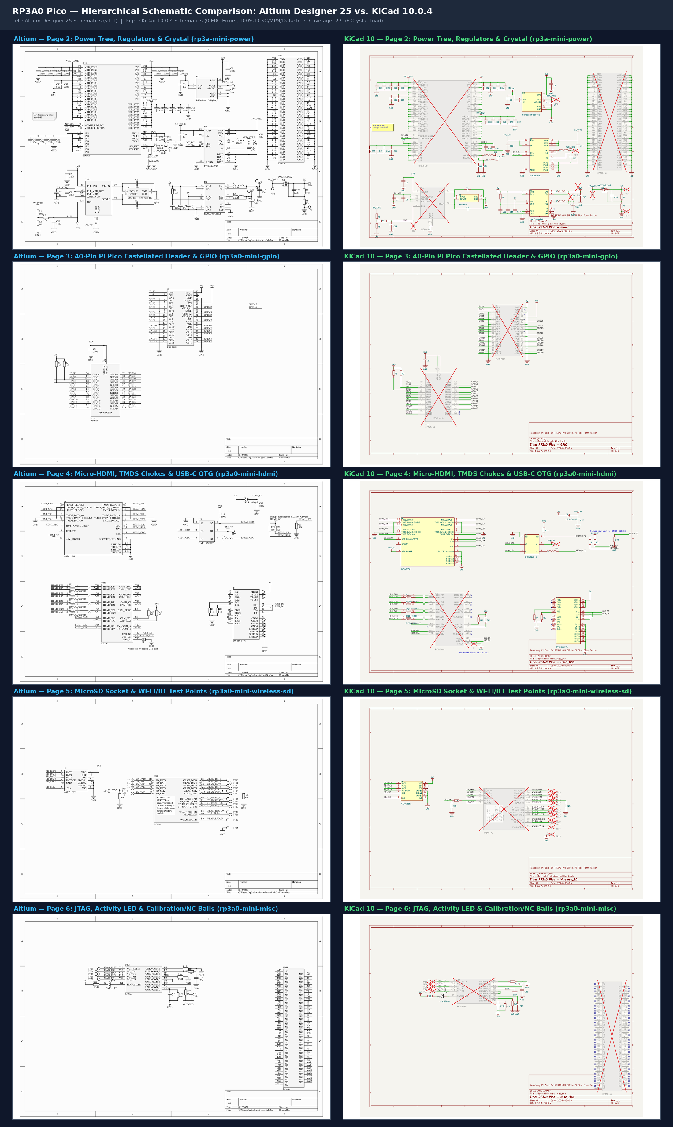
| Sheet Name | File | Contents |
|---|---|---|
Root | rp3a0-mini.kicad_sch | Top-level hierarchical sheet linking the 5 functional subsheets |
Power | rp3a-mini-power.kicad_sch | U4 (PAM2306AYPKE), U3 (RT8088AWSC), U2 (NCP133AMX125TCG), Q1 (DMG2305UX-7), Y1 (19.2 MHz crystal with 30 pF load caps C6, C9), decoupling, and U1 Power/GND/PLL units |
GPIO | rp3a0-mini-gpio.kicad_sch | U1 GPIO bank (GPIO0–GPIO27), I2C pull-ups (R1, R2), and 40-pin Raspberry Pi Pico castellated edge header (J5) |
HDMI_USB | rp3a0-mini-hdmi.kicad_sch | Micro-HDMI (J2), TMDS common-mode chokes (FL1–FL4), CEC/HPD level shifter (U5, DMN601VK-7), Schottky diode (D2), USB-C (J3), and USB_ID jumper (J4) |
Wireless_SD | rp3a0-mini-wireless-sd.kicad_sch | MicroSD card slot (J1), SD_CLK termination (R14, R15), and top-side Wi-Fi SDIO / Bluetooth UART test points (TP10–TP22, TP28) |
Misc_JTAG | rp3a0-mini-misc.kicad_sch | JTAG test points (TP23–TP27), activity LED (D1 KT-0603G, R11), calibration resistors (R12, R13, R16, R17, R18), and 86 NC balls |
build/gerbers.zip, select 6 Layers, 1.6 mm thickness, Green solder mask, ENIG surface finish, Castellated Holes: Yes (2 edges), and Panel by JLCPCB (with 5 mm tooling rails and routed tabs) for Standard PCBA.jlcpcb/rp3a0-mini-bom.csv and jlcpcb/rp3a0-mini-cpl.csv, select Top Side Only (93 SMT parts across 37 BOM lines). Pre-order / Global-Source U2 (C603545), U3 (C5739348), and J2 (C6961796) into your JLCPCB Parts Library prior to assembly checkout; U1 (RP3A0-AU) is marked DNP and hand-reflowed after harvesting/reballing from a donor Raspberry Pi Zero 2W.make)make all — Run PyTest verification suite, DRC, and ERC.make test — Run 16 automated hardware verification tests in tests/test_pcb.py.make erc / make drc — Run kicad-cli schematic ERC and 6-layer PCB DRC with zone refill and schematic parity.make fab — Execute export_manufacturing.py --all to generate build/gerbers/, build/gerbers.zip, build/rp3a0-mini-bom.csv/.xlsx, build/rp3a0-mini-cpl.csv/.xlsx, build/rp3a0-mini.d356, build/rp3a0-mini_Schematic.pdf, build/rp3a0-mini_PCB_Layers.pdf, build/ORDER_SPEC.md, and build/rp3a0-mini_JLCPCB_Release.zip.| Qty | Value | Footprint | References |
|---|---|---|---|
| 28 | 220n | rp3a0:0402 | C1, C2, C18, C20, C21, C22, C23, C24, C26, C27, C28, C29, C30, C31, C32, C33 +12 |
| 28 | TEST_POINT | rp3a0:TEST_POINT_1.2MM | TP1, TP2, TP10, TP11, TP12, TP13, TP14, TP15, TP16, TP17, TP18, TP19, TP20, TP21, TP22, TP23 +12 |
| 6 | 1.8k | rp3a0:RES-0402-SML | R1, R2, R21, R22, R23, R24 |
| 6 | 10u | rp3a0:0603 | C3, C4, C11, C13, C16, C17 |
| 4 | EXC24CH900U | rp3a0:FIL_EXC24CB102U | FL1, FL2, FL3, FL4 |
| 3 | 100k | rp3a0:RES-0402-SML | R3, R19, R20 |
| 3 | 100n | rp3a0:0402 | C15, C19, C47 |
| 3 | 220R | rp3a0:0402 | L4, L5, L6 |
| 3 | 240R | rp3a0:RES-0402-SML | R12, R13, R18 |
| 3 | 4.7u | rp3a0:0603 | C36, C38, C43 |
| 3 | 47k | rp3a0:RES-0402-SML | R7, R15, R25 |
| 2 | 1u | rp3a0:0402 | C7, C10 |
| 2 | 30p | rp3a0:0402 | C6, C9 |
| 2 | 47u | rp3a0:C0805_NP | C12, C14 |
| 2 | 5.1k | rp3a0:RES-0402-SML | R9, R10 |
| 1 | 100p | rp3a0:0402 | C25 |
| 1 | 1054500101 | rp3a0:MOLEX_105450-0101 | J3 |
| 1 | 10k | rp3a0:RES-0402-SML | R6 |
| 1 | 18k | rp3a0:RES-0402-SML | R8 |
| 1 | 19.2MHz | rp3a0:XTAL_ECS-192-18-33-JGN-TR | Y1 |
| 1 | 1k | rp3a0:RES-0402-SML | R17 |
| 1 | 2.2uH | rp3a0:INDP2622X120N | L3 |
| 1 | 3.9k | rp3a0:RES-0402-SML | R16 |
| 1 | 33R | rp3a0:RES-0402-SML | R14 |
| 1 | 4.7uH | rp3a0:INDP4040X180N | L2 |
| 1 | 467652301 | rp3a0:MOLEX_467652301 | J2 |
| 1 | 470R | rp3a0:RES-0402-SML | R11 |
| 1 | 470k | rp3a0:RES-0402-SML | R4 |
| 1 | 470nH | rp3a0:INDC2016X100N | L1 |
| 1 | 473092651 | rp3a0:MOLEX_0475710001 | J1 |
| 1 | 82k | rp3a0:RES-0402-SML | R5 |
| 1 | DFLS130L-7 | rp3a0:DIO_DFLS130LQ-7 | D2 |
| 1 | DMG2305UX-7 | rp3a0:SOT91P240X110-3N_DMG2305UX-7 | Q1 |
| 1 | DMN601VK-7 | rp3a0:SOT50P162X60-6N | U5 |
| 1 | LED_GREEN | rp3a0:LED_0603 | D1 |
| 1 | NCP133AMX125TCG | rp3a0:VREG_RT9081A_1BGQZA_2 | U2 |
| 1 | PAM2306AYPKE | rp3a0:SON45P300X300X80-13N | U4 |
| 1 | PICO_PADS | rp3a0:PICO_PADS | J5 |
| 1 | RP3A0-AU | rp3a0:RP3A0-BGA | U1 |
| 1 | RT8088AWSC | rp3a0:15B_WLCSP_1.31X2.11 | U3 |
| 1 | SOLDER_PAD_OPEN | rp3a0:SOLDER_PAD_OPEN | J4 |

dubnubdubnub/Giris
open source 32 key/half (64 total) analog TMR split ortholinear keyboard w/ 8kHz USB HS


sabogalc/project-piCo
Because it should be a crime to release a product with Micro-USB in the 2020s

nikolajevs/PCB_EU
Сохраняются функции PCBV1: два LED-канала с общей яркостью, два независимых PWM/тахоканала вентиляторов, PTC, помпа, SHT4x, поплавок, RTC с CR2032, microSD, Wi-Fi и существующие функции интерфейса/расписаний.

It measures 60 × 20.4 mm and has 6 copper layers, 1.62 mm thick.
124 parts, built around the PAM2306AYPKE, RT8088AWSC, EXC24CH900U and 0402CG300J500NT. The full list of its parts is on this page, with links to each part's symbol and footprint where PCBKit's library has them.
From the CopperPilot/rpi-zero-2w-kicad repository on GitHub, at the commit this page was made from: the board is pcb/rp3a0-mini.kicad_pcb and its schematic pcb/rp3a-mini-power.kicad_sch. PCBKit opens the board in the browser, with nothing to install.
Its repository states no licence, so its author keeps all rights: ask CopperPilot before reusing the design.