2 layers97.2 × 59.1 mm
ArmLEDsPrototype
hackclub/OnBoard
💡 Join 1,000 teenagers and make your first PCB with a $100 grant!
35 parts915

 ColinVanderMeer/Cynboard
Hackpad is an open-source printed circuit board by ColinVanderMeer, from the ColinVanderMeer/Cynboard repository on GitHub. It is a 2-layer board of 79.5 × 100 mm with 35 parts on 30 nets, routed with 131 tracks and 0 vias.
Its parts include 16 diodes, 16 switches and 2 ICs. It belongs with the RP2040 boards of this library.
This is my submission for Hack Club Blueprint / sorta Hackpad V5. Thanks Cyaopad for serving as my go to board to look at when I had a problem.
| Schematic | PCB |
|---|---|
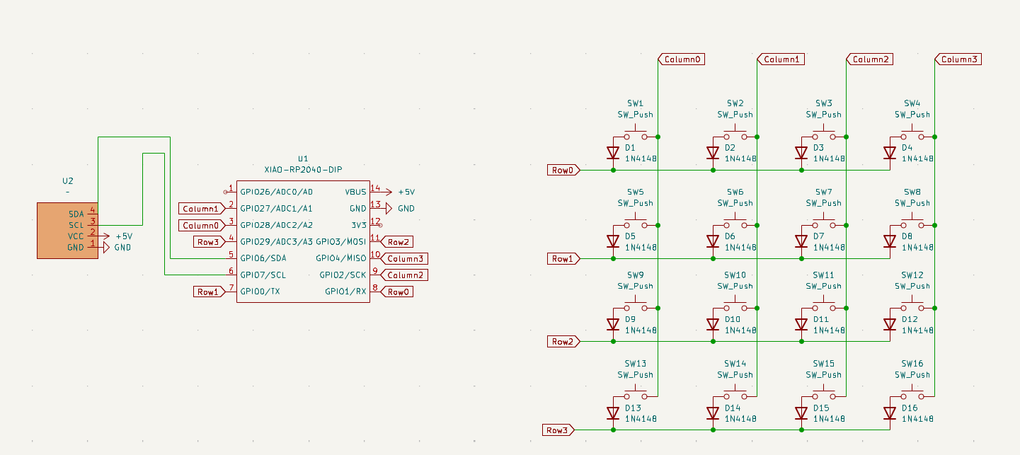 | 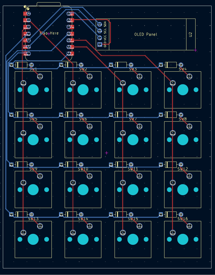 |
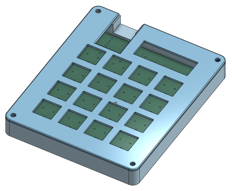
| Qty | Value | Footprint | References |
|---|---|---|---|
| 16 | 1N4148 | Diode_THT:D_DO-35_SOD27_P7.62mm_Horizontal | D1, D2, D3, D4, D5, D6, D7, D8, D9, D10, D11, D12, D13, D14, D15, D16 |
| 16 | SW_Push | Button_Switch_Keyboard:SW_Cherry_MX_1.00u_PCB | SW1, SW2, SW3, SW4, SW5, SW6, SW7, SW8, SW9, SW10, SW11, SW12, SW13, SW14, SW15, SW16 |
| 1 | LOGO | LOGO | G*** |
| 1 | XIAO-RP2040-DIP | OPL:XIAO-RP2040-DIP | U1 |
| 1 | ~ | oled:SSD1306-0.91-OLED-4pin-128x32 | U2 |
hackclub/OnBoard
💡 Join 1,000 teenagers and make your first PCB with a $100 grant!


ozel/DIY_particle_detector
A mobile low-cost spectrometer for measuring radioactivity and the energy of ionising radiation like alpha particles and electrons

Seeed-Studio/OSHW-reCamera-Series
reCamera is a series of open-source AI cameras.


It measures 79.5 × 100 mm and has 2 copper layers, 1.6 mm thick.
35 parts. The full list of its parts is on this page, with links to each part's symbol and footprint where PCBKit's library has them.
From the ColinVanderMeer/Cynboard repository on GitHub, at the commit this page was made from: the board is PCB/hackpad.kicad_pcb and its schematic PCB/Lib/OPL_Kicad_Library-master/Grove Vision AI V2 Library/Grove - Vision AI Module V2.kicad_sch. PCBKit opens the board in the browser, with nothing to install.
Its repository states no licence, so its author keeps all rights: ask ColinVanderMeer before reusing the design.