
4 layers65 × 56.5 mm
LEGHAT
Chairwheels/LEGHAT
This project was done in KiCad as I found it easier to work in and had more support throughout the industry as it is second in use only to Altium designer for PCB design tools.
5 parts
 Chairwheels/LEGHAT
This project was done in KiCad as I found it easier to work in and had more support throughout the industry as it is second in use only to Altium designer for PCB design tools.
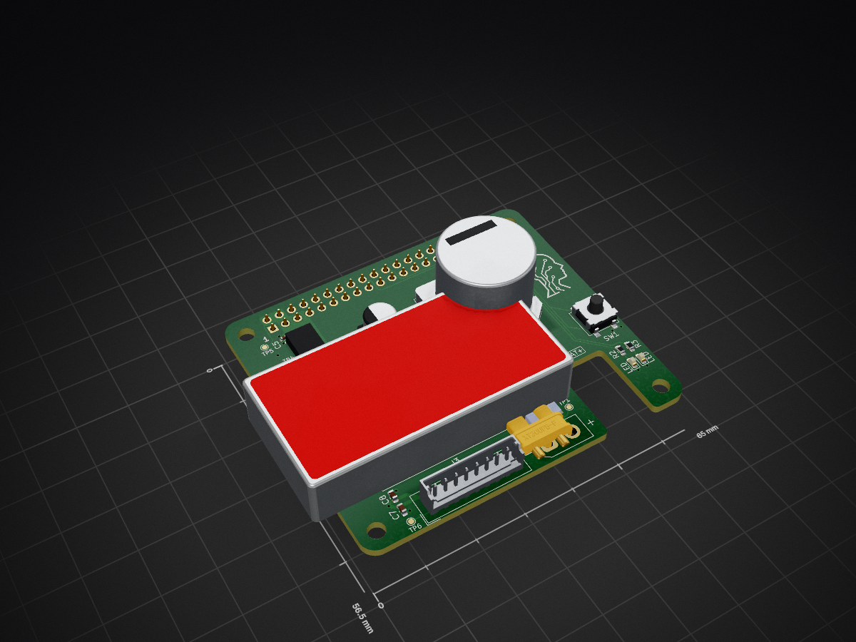
LEGHAT+ is an open-source printed circuit board by Chairwheels, from the Chairwheels/LEGHAT repository on GitHub. It is a 4-layer board of 65 × 56.5 mm with 34 parts on 44 nets, routed with 177 tracks and 37 vias.
It is built around the CSD18540Q5B. Its parts include 7 capacitors, 4 diodes, 3 resistors, 3 connectors and 1 IC.
This project was done in KiCad as I found it easier to work in and had more support throughout the industry as it is second in use only to Altium designer for PCB design tools.
Design a four-layer Raspberry Pi 5 HAT that powers the Pi through its 40-pin header from a 33.3–37.8 V battery instead of its USB-C power input. The board uses an isolated DC/DC converter, input protection, and a MOSFET-based backfeed protection. It also breaks out SPI for two encoders and a load-cell data-acquisition (DAQ) board, and includes a pushbutton and two LEDs for either USB or PI Shutdown.
The designators below follow the current schematic and parts list.
| PCB designation | Part / selection | Function |
|---|---|---|
| J1 | Raspberry Pi 40-pin header; Samtec SSW-120-01-F-D | Connects power, ground, SPI, and control signals to the Pi GPIO header. |
| J2 | AMASS XT30UPB-F | Battery input connector. |
| F1 | Bel Fuse 0680L3000-05, 3 A | Input overcurrent protection |
| D1 | Vishay SS5P10-M3/86A | Series Schottky diode for input reverse polarity protection. |
| D2 | Vishay SMCJ43A-E3/57T | TVS diode for input transient suppression. |
| C1 | Samsung CL31B105KCHNNNE, 1 µF | High frequency bypass on the battery/converter input. |
| C2 | Panasonic EEEFK2A221AM, 220 µF | Battery side bulk input capaciter. |
| PS1 | TRACO Power THN 30-4811WI | Isolated DC/DC converter from battery voltage to the low-voltage rail. |
| R1 | Panasonic ERJPB3B4992V, 49.9 kΩ | Fixed resistor in the converter trim network. |
| RV1 | Bourns 3224W-1-204E, 200 kΩ | Adjustable resistor in the converter trim network. |
| C3 | Samsung CL32B226KAJNNNE, 22 µF | Converter output capacitance before the backfeed protection stage. |
| Q2 | Texas Instruments CSD18540Q5B | MOSFET in the backfeed protection stage. |
| U4 | Analog Devices LTC4373IDD#PBF | Ideal diode controller for the MOSFET backfeed protection stage. |
| C4 | TDK C1005X7R1E104KT000F, 100 nF | Local bypass capacitor for U4. |
| C5 | Panasonic 16SVPC100M, 100 µF | Bulk capacitance on the protected HAT_5V0 output. |
| J3 | Molex 55932-0810, 8-circuit MicroClasp header | Peripheral connector for 3.3 V, ground, SPI clock/data, and chip-select signals. |
| C7 | Vishay VJ0603Y104JXQCW1BC, 100 nF | High frequency decoupling for the peripheral 3.3 V supply near J3. |
| C8 | Samsung CL10B105KP8NNNC, 1 µF | Local decoupling for the peripheral 3.3 V supply near J3. |
| SW1 | Omron B3SL-1022P | Pushbutton for the planned shutdown interface. |
| D3 | Lite-On LTST-C191KGKT, green LED | Green status indicator (GREEN_LED). |
| D4 | Lite-On LTST-C191KRKT, red LED | Red status indicator (RED_LED). |
| R2, R3 | Yageo AC0603FR-07470RL, 470 Ω | Current limiting resistors for the green and red LEDs. |
Bat_Neg. D2, C1, and C2 are connected across the battery side input as shown in the schematic.HAT_5V0 and feeds the Pi header at J1 pins 2 and 4.This table records the signal order shown in the current schematic. It is the pinout for the molex connector. The OSL pinouts were used as reference.
| J3 pin | Net | Purpose |
|---|---|---|
| 1 | HAT_3.3V | 3.3 V peripheral supply |
| 2 | SPI1_CSn2 | SPI1 chip-select net 2 |
| 3 | SPI1_CSn1 | SPI1 chip-select net 1 |
| 4 | SPI1_CSn0 | SPI1 chip-select net 0 |
| 5 | SPI1_SCLK | SPI clock |
| 6 | SPI1_MISO | Pi-to-peripheral data return (peripheral output) |
| 7 | SPI1_MOSI | Pi-to-peripheral data (Pi output) |
| 8 | HAT_GND | Pi-side ground reference |
The two encoders and the DAQ share SPI1_SCLK, SPI1_MOSI, and SPI1_MISO. Each device uses its own chip-select. The load cell connects to the DAQ, then to the Pi.
The Pi header assignments below use the standard Raspberry Pi 40-pin header pinout and the SPI1 mapping.
| J1 pin | Intended net / signal | Purpose |
|---|---|---|
| 1, 17 | HAT_3.3V | 3.3 V rail for peripheral logic |
| 2, 4 | HAT_5V0 | Protected 5 V supply to the Pi |
| 6, 9, 14, 20, 25, 30, 34, 39 | HAT_GND | Pi-side ground |
| 11 | SPI1_CSn1 | SPI1 chip select 1 / GPIO17 |
| 12 | SPI1_CSn0 | SPI1 chip select 0 / GPIO18 |
| 18 | GREEN_LED | Green LED control / GPIO24 |
| 22 | RED_LED | Red LED control / GPIO25 |
| 35 | SPI1_MISO | SPI1 MISO / GPIO19 |
| 36 | SPI1_CSn2 | SPI1 chip select 2 / GPIO16 |
| 37 | PWR_Switch | Shutdown button signal / GPIO26 |
| 38 | SPI1_MOSI | SPI1 MOSI / GPIO20 |
| 40 | SPI1_SCLK | SPI1 clock / GPIO21 |
The SPI1 mapping follows the Raspberry Pi documentation: CE0 on physical pin 12, CE1 on pin 11, CE2 on pin 36, MISO on pin 35, MOSI on pin 38, and SCLK on pin 40. The SPI1_CSn0, SPI1_CSn1, and SPI1_CSn2 nets on J1 should connect to the corresponding chip-select signals on J3.
The PCB includes six numbered test points to simplify power testing and troubleshooting. Ground measurement references are provided by vias connected to the appropriate ground planes.
| Test Point | Net | PCB Location | Purpose |
|---|---|---|---|
| TP1 | J2-Pin_2 | At J2's battery connection before F1 | Measures the battery voltage before the fuse and input protection. |
| TP2 | D1-K (On D1) | Between F1 and D1 | Measures if the battery voltage passes through the input fuse. |
| TP3 | D1-K (On C1 | After D1, near the positive input pin of PS1 | Measures the voltage reaching the TRACO DC/DC converter after input protection. |
| TP4 | PS1-+VOUT | At the converter output, near C3 and the converter-side terminal of Q2 | Measures the converter output before the MOSFET backfeed protection. |
| TP5 | HAT_5V0 | On the protected side of Q2, near C5 and J1 | Measures the final 5 V supply delivered to the Raspberry Pi. |
| TP6 | HAT_3.3V | Near J3 pin 1, on the peripheral 3.3 V supply | Makes sure the MOLEX connector receives its 3.3 V supply from the Raspberry Pi. |
Two separate ground reference vias are used for measurements:
BAT_NEG via: Located between TP1 and D1. Use this as the reference when measuring TP1, TP2, and TP3.HAT_GND via: Located between TP4 and TP5 near HAT_5V0 net. Use this as the reference when measuring TP4, TP5, and TP6.| Qty | Value | Footprint | References |
|---|---|---|---|
| 6 | TestPoint | TestPoint:TestPoint_Pad_D1.0mm | TP1, TP2, TP3, TP4, TP5, TP6 |
| 4 | MountingHole 3.2mm | MountingHole:MountingHole_3.2mm_M3_DIN965 | H1, H2, H3, H4 |
| 2 | C | Capacitor_SMD:C_0603_1608Metric | C7, C8 |
| 2 | LED | LED_SMD:LED_0603_1608Metric | D3, D4 |
| 2 | R | Resistor_SMD:R_0603_1608Metric | R2, R3 |
| 1 | 100nF | Capacitor_SMD:CP_Elec_6.3x5.8 | C4 |
| 1 | 100uF 16V | Capacitor_SMD:C_0402_1005Metric | C5 |
| 1 | 1uF 100V | Capacitor_SMD:C_1206_3216Metric | C1 |
| 1 | 200k | Potentiometer_SMD:Potentiometer_Bourns_3224W_Vertical | RV1 |
| 1 | 220uF 100V | EEE-FK2A221AM-SM:CAP_EEEFK2A221AM | C2 |
| 1 | 22uF 25V | Capacitor_SMD:C_1210_3225Metric | C3 |
| 1 | 49.9k | Resistor_SMD:R_0603_1608Metric | R1 |
| 1 | CSD18540Q5B | ul_CSD18540Q5B:DNK0008A | Q2 |
| 1 | Conn_01x02 | Connector_AMASS:AMASS_XT30UPB-F_1x02_P5.0mm_Vertical | J2 |
| 1 | Conn_01x08 | Connector_Molex:Molex_MicroClasp_55932-0810_1x08_P2.00mm_Vertical | J3 |
| 1 | Conn_02x20_Odd_Even | Connector_PinSocket_2.54mm:PinSocket_2x20_P2.54mm_Vertical | J1 |
| 1 | D_Schottky_AAK | Package_TO_SOT_SMD:TO-277A | D1 |
| 1 | D_Zener | Diode_SMD:D_SMC | D2 |
| 1 | Fuse | belfuse0680L3000-05:FUSC6125X279N | F1 |
| 1 | LOGO | BoardDewsign:logogo | G*** |
| 1 | LTC4373IDD-PBF | LTC4373IDD-PBF:DFN8_DD_05-08-1698_ADI | U4 |
| 1 | SW_Push | Button_Switch_SMD:SW_SPST_B3SL-1022P | SW1 |
| 1 | THN_30-4811WI | Converter_DCDC:Converter_DCDC_TRACO_THN30-xxxx_THT | PS1 |
Chairwheels/LEGHAT
This project was done in KiCad as I found it easier to work in and had more support throughout the industry as it is second in use only to Altium designer for PCB design tools.

azmat-bilal/bldc_motor_controller_pcb
A Brushless DC Motor controller board. The design is inspired and is compatible with Odrive project (https://github.com/madcowswe/ODriveHardware) except that this one has a single channel.


Kaiser041224/HPM5361-RMCS_Slave-Pro
HPM5361-RMCSSlave-V1.0 是一个基于 KiCad 9 的硬件工程,核心主控为 HPM5361ICB1。从顶层框图、层级原理图和关键器件选型来看,这块板更像一块面向机器人/运动控制场景的从控板,用于通信汇聚、PWM 外设输出、姿态感知、板载存储和基础人机交互。


Kaiser041224/HPM5361-RMCS_Slave-Lite
HPM5361-RMCSSlave-Lite 是一个基于 HPM5361IEG1 的嵌入式控制板。以下说明是根据当前 KiCad 工程中的原理图层级、器件选型和 PCB 丝印整理出来的硬件简介;从接口组合来看,这块板更像是一个面向机器人或分布式控制系统的从控/通信节点。
It measures 65 × 56.5 mm and has 4 copper layers, 1.62 mm thick.
34 parts, built around the CSD18540Q5B. The full list of its parts is on this page, with links to each part's symbol and footprint where PCBKit's library has them.
From the Chairwheels/LEGHAT repository on GitHub, at the commit this page was made from: the board is HATPlus/LEGHAT+.kicad_pcb and its schematic HATPlus/LEGHAT+.kicad_sch. PCBKit opens the board in the browser, with nothing to install.
Its repository states no licence, so its author keeps all rights: ask Chairwheels before reusing the design.