
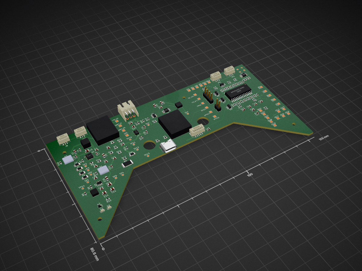
2 layers155 × 80.6 mm
Daughterboard before add j30 5v uart pad
BoomBoxRobotics/Anubis
Anubis is a project to create the ultimate open source RC controller utilizing inexpensive consumer parts and clever programming.
148 parts2CC0-1.0
 BoomBoxRobotics/Anubis2
Anubis is a project to create the ultimate open source RC controller utilizing inexpensive consumer parts and clever programming.
Daughterboard.pre r14 csd18502 swap is an open-source printed circuit board by BoomBoxRobotics, from the BoomBoxRobotics/Anubis repository on GitHub, published under the CC0-1.0 licence. It is a 4-layer board of 155 × 80.6 mm with 166 parts on 103 nets, routed with 1,267 tracks and 198 vias.
It is built around the BQ28Z610DRZR-R1. Its parts include 50 resistors, 33 capacitors, 21 connectors, 6 ICs and 6 diodes.
A compact open-hardware support board for a DIY ESP32-S3 RC transmitter.
Anubis is an open hardware and open firmware RC controller project built around accessible DIY parts, modern radio-control features, and a design that builders can understand, repair, modify, and improve.
This repository contains the custom daughterboard for the Anubis controller. It sits under a Hosyond 2.8 inch ESP32-S3 display board and turns the early wiring-heavy prototype into a cleaner, more repeatable hardware platform.
The goal is simple: make a capable, repairable, hackable transmitter that is not locked behind a black box.
The first Anubis prototype used off-the-shelf modules wired together by hand: display board, power switches, regulators, analog input boards, GPIO expanders, gimbal connectors, and radio wiring. That is a great way to prove an idea, but it gets messy fast. This daughterboard pulls those support circuits onto a purpose-built PCB while leaving the Hosyond ESP32-S3 board as the main brain, display, touch interface, and firmware target.
Anubis is meant for experimentation as much as use. Builders should be able to change pin mappings, adapt connectors, swap radio hardware, and tune the firmware for their own transmitter layout.
| Area | Current Direction |
|---|---|
| Main controller | Hosyond 2.8 inch ESP32-S3 display/dev board |
| Battery system | 2S LiPo or two 18650 cells as a 2S pack |
| Charging input | USB-C 5 V input, 500 mA to 1.5 A charge target |
| Switched outputs | +5V_SW and +3V3_SW accessory rails |
| Analog inputs | Two onboard ADS1115 ADCs, up to 8 analog channels |
| GPIO expansion | MCP23017 16-bit I2C GPIO expander |
| Radio paths | ELRS/CRSF over UART and optional ESP-NOW |
| Assembly goal | As much JLCPCB assembly as practical |
| Project status | Prototype hardware, ready for assembled-board validation |
The daughterboard adds the support electronics around the Hosyond ESP32-S3 board:
BQ28Z610DRZR-R1.CSD18502Q5B N-FETs, with the charger and buck regulators fed from protected BAT_SYS.| Rail | Intended Use | Approximate Max Current |
|---|---|---|
| USB-C input | 5 V charge/input source | 500 mA to 1.5 A charge target |
+5V_SW | ELRS/UART-side accessory power | about 1 A |
+3V3_SW | I2C, ADCs, MCP23017, gimbals, sensors | about 500 mA |
The switched rails are controlled through the two Pololu #2808 mini pushbutton power switch modules. The ESP32-S3 can shut down attached devices without relying on the attached devices to behave nicely.
The main Anubis firmware runs on the Hosyond ESP32-S3 board. Current daughterboard-aware firmware support includes:
0x48 and 0x49.0x20.| Function | ESP32-S3 Pin |
|---|---|
| I2C SDA | GPIO16 |
| I2C SCL | GPIO15 |
| ELRS/UART TX | GPIO44 |
| ELRS/UART RX | GPIO43 |
| Battery ADC | GPIO9 |
| 5 V rail switch control | GPIO2 |
| 3.3 V rail switch control | GPIO3 |
| Deep-sleep/wake button sense | GPIO14 |
| Deep-sleep/wake button reference | GPIO21 |
GPIO2 and GPIO3 control the two Pololu rail-switch modules. GPIO14 and GPIO21 route to the two-pin deep-sleep/wake pushbutton header. UART-to-ELRS wiring can still be crossed manually if a specific module harness expects the opposite order.
| Device | Address | Role |
|---|---|---|
| ADS1115 primary | 0x48 | Four gimbal/stick analog axes |
| ADS1115 auxiliary | 0x49 | Spare analog inputs |
| MCP23017 | 0x20 | GPIO expansion and active-low button/switch inputs |
| BQ25887 charger | 0x6B | 2S charger status and pack voltage reporting |
The following tables describe the designators and nets on the R14 PCB. Pin numbers are the KiCad footprint pin numbers and should be checked against connector orientation and pin-1 markings before making a cable.
| Pad | Net | Signal source or intended measurement |
|---|---|---|
TP1 | USB_VBUS | USB-C J1 VBUS, before input fuse F1 |
TP2 | CHG_IN | Fused USB input after F1; charger U1 pin 23 |
TP3 | BAT_SYS | Protected battery/system bus feeding charger U1 BAT pins and the 5 V/3.3 V regulators |
TP4 | CELL_MID | 2S pack midpoint from J7 pin 2; charger U1 pin 9 sense connection |
TP5 | BAT_SYS | Second protected battery/system-bus test point; electrically the same as TP3 |
TP6 | +5V | Unswitched 5 V regulator output after L1, before Pololu switch SW1 |
TP7 | +3V3 | Unswitched 3.3 V regulator output after L2, before Pololu switch SW2 |
TP9 | +3V3_SW | Switched 3.3 V output from SW2 |
TP10 | CHG_STAT | Charger U1 pin 2 charge-status output; also drives status LED D2 |
TP11 | PG_STAT | Charger U1 pin 1 power-good output; also drives status LED D3 |
TP12 | BATT_RAW_N | Raw pack negative from J7 pin 1, on the battery side of current-sense resistor R46 |
TP13 | BATT_RAW_P | Raw pack positive from J7 pin 3 |
TP14 | GND | System ground, on the system side of current-sense resistor R46 |
TP15 | AIN4 | Auxiliary ADC U6 (0x49) AIN0, pin 4 |
TP16 | AIN5 | Auxiliary ADC U6 (0x49) AIN1, pin 5 |
TP17 | AIN6 | Auxiliary ADC U6 (0x49) AIN2, pin 6 |
TP18 | AIN7 | Auxiliary ADC U6 (0x49) AIN3, pin 7 |
TP8 is not fitted on the R14 PCB. Use J30 or J4 pin 1 to access +5V_SW. Also note that BATT_RAW_N and GND are separated by the 2 mOhm current-sense resistor; do not treat TP12 and TP14 as interchangeable measurement points.
These pads replace the original J3 connector so individual wires from the Hosyond board can be soldered directly to the daughterboard.
| Pad | Net | Hosyond/source mapping |
|---|---|---|
J30 | +5V_SW | Switched 5 V output from SW1; also available at J4 pin 1 |
J31 | UART_TX | Hosyond ESP32-S3 GPIO44; routed to J4 pin 3 |
J32 | UART_RX | Hosyond ESP32-S3 GPIO43; routed to J4 pin 4 |
J33 | I2C_SDA | Hosyond ESP32-S3 GPIO16; shared daughterboard I2C data bus |
J34 | I2C_SCL | Hosyond ESP32-S3 GPIO15; shared daughterboard I2C clock bus |
J35 | GPIO2 | Hosyond ESP32-S3 GPIO2; drives SW1 5 V control through R17 |
J36 | GPIO3 | Hosyond ESP32-S3 GPIO3; drives SW2 3.3 V control through R18 |
J37 | GPIO14 | Hosyond ESP32-S3 GPIO14; routed to wake-button header J6 pin 1 |
J38 | GPIO21 | Hosyond ESP32-S3 GPIO21; routed to wake-button header J6 pin 2 |
J39 | GND | Daughterboard system ground |
The EXP_* GPIO pads are on the protected external side of a 100 ohm series resistor and an ESD array. U7 is the MCP23017 at I2C address 0x20.
| Pad | Net | Source |
|---|---|---|
J91 | EXP_GPA0 | U7 GPA0 pin 21 through R23; ESD D4 |
J92 | EXP_GPA1 | U7 GPA1 pin 22 through R24; ESD D4 |
J93 | EXP_GPA2 | U7 GPA2 pin 23 through R25; ESD D4 |
J94 | EXP_GPA3 | U7 GPA3 pin 24 through R26; ESD D4 |
J95 | EXP_GPA4 | U7 GPA4 pin 25 through R27; ESD D5 |
J96 | EXP_GPA5 | U7 GPA5 pin 26 through R28; ESD D5 |
J97 | EXP_GPA6 | U7 GPA6 pin 27 through R29; ESD D5 |
J98 | EXP_GPA7 | U7 GPA7 pin 28 through R30; ESD D5 |
J99 | EXP_GPB0 | U7 GPB0 pin 1 through R31; ESD D6 |
J910 | EXP_GPB1 | U7 GPB1 pin 2 through R32; ESD D6 |
J911 | EXP_GPB2 | U7 GPB2 pin 3 through R33; ESD D6 |
J912 | EXP_GPB3 | U7 GPB3 pin 4 through R34; ESD D6 |
J913 | EXP_GPB4 | U7 GPB4 pin 5 through R35; ESD D7 |
J914 | EXP_GPB5 | U7 GPB5 pin 6 through R36; ESD D7 |
J915 | EXP_GPB6 | U7 GPB6 pin 7 through R37; ESD D7 |
J916 | EXP_GPB7 | U7 GPB7 pin 8 through R38; ESD D7 |
J925 | MCP_INTA | U7 INTA pin 20 with pull-up R43 |
J926 | MCP_INTB | U7 INTB pin 19 with pull-up R44 |
J927 | MCP_RESET | U7 RESET pin 18 with pull-up R42 and capacitor C29 |
J928 | +3V3_SW_LOGIC | Switched 3.3 V logic rail after isolation link R45 |
J929 | GND | Daughterboard system ground |
| Connector | Purpose | Pinout |
|---|---|---|
J1 | USB-C 5 V input | A5 = CC1; B5 = CC2; A9/B9 = USB_VBUS; A12/B12 = GND; shield tabs = GND |
J4 | 5-pin UART JST-GH, top-entry, 1.25 mm | 1 = +5V_SW; 2 = GND; 3 = UART_TX; 4 = UART_RX; 5 = GND |
J5 | 4-pin I2C through-hole header, 2.54 mm | 1 = +3V3_SW; 2 = GND; 3 = I2C_SDA; 4 = I2C_SCL |
J6 | 2-pin deep-sleep/wake button header, 2.54 mm | 1 = GPIO14; 2 = GPIO21; a momentary button connects the two pins |
J7 | 2S balance input, side-entry JST-XH, 2.50 mm | 1 = BATT_RAW_N; 2 = CELL_MID; 3 = BATT_RAW_P |
J8 | Left gimbal A, 3-pin JST-GH, 1.25 mm | 1 = GND; 2 = AIN0; 3 = +3V3_SW |
J40 | Left gimbal B, 3-pin JST-GH, 1.25 mm | 1 = GND; 2 = AIN1; 3 = +3V3_SW |
J41 | Right gimbal A, 3-pin JST-GH, 1.25 mm | 1 = GND; 2 = AIN2; 3 = +3V3_SW |
J42 | Right gimbal B, 3-pin JST-GH, 1.25 mm | 1 = GND; 2 = AIN3; 3 = +3V3_SW |
J2 is a schematic-only switched-power-output symbol and has no footprint on the R14 PCB. J3 is not a physical connector; its signals are implemented as solder pads J30 through J39. JST-GH mounting pads marked MP are mechanical and have no electrical connection.
| Header | Pin 1 | Pin 2 | Pin 3 | Pin 4 |
|---|---|---|---|---|
SW1 Pololu #2808 5 V switch | +5V input | +5V_SW output | GND | CTRL_5V_SW |
SW2 Pololu #2808 3.3 V switch | +3V3 input | +3V3_SW output | GND | CTRL_3V3_SW |
The controller is designed around parts that are easy for hobby builders to source or substitute:
The mechanical layout fits around the Hosyond board and controller shell constraints. The Hosyond board sits above the daughterboard on standoffs, with the daughterboard occupying the surrounding and lower internal space.
| Path | Purpose |
|---|---|
Daughterboard.kicad_pro | KiCad project file |
Daughterboard.kicad_sch | Main schematic |
Daughterboard.kicad_pcb | PCB layout |
Daughterboard.kicad_sym | Project symbols |
Daughterboard.pretty/ | Custom KiCad footprints |
Daughterboard.net | Exported netlist |
Daughterboard_pcb_bom.csv | Human-readable PCB BOM |
Daughterboard_current_jlc_part_audit.csv | JLC part audit/reference |
fabrication/ | Fabrication and assembly outputs |
daughterboard2.dxf | Board outline reference |
Daughterboardv2.step | Mechanical board reference |
PROJECT_CONTEXT.md | Detailed working context for future development |
Current fabrication package:
fabrication/jlcpcb_2026-07-10_r14.zipAssembly files are included under:
fabrication/jlcpcb_2026-07-10_r14/assembly/The board is being prepared for JLCPCB assembly with as many populated parts as practical. The Pololu mini pushbutton power switch modules are treated as separately installed modules. Some through-hole headers may also be hand-installed unless through-hole assembly is explicitly ordered.
Before ordering boards, always check:
Known current status from the active R14 working files:
CSD18502Q5B FETs using project-local TI DNK/VSON-CLIP footprints.R49 and R50.This board works with lithium battery packs and charging/protection circuitry. Mistakes can damage hardware or create a safety hazard.
Do not assume a PCB revision is safe just because the schematic opens or the Gerbers generate. Review the battery path, charger configuration, protection FETs, current limits, connector polarity, and pack wiring before connecting real cells.
Use protected cells or a known-good 2S pack during testing. Current-limit the first power-up and verify rails with a meter before plugging in the Hosyond board or radio hardware.
This hardware is still a prototype until assembled boards are tested.
Open work includes:
Anubis is meant to be community driven. Contributions are welcome in the form of firmware changes, PCB review, mechanical improvements, documentation, testing notes, alternate part suggestions, and build reports.
If you change the hardware, include enough context for another builder to understand why the change was made. If you change the firmware, document the pin assumptions and hardware revision you tested against.
The firmware and receiver-side code for the broader Anubis controller project are hosted with the main project:
https://github.com/BoomBoxRobotics/AnubisThis daughterboard is one hardware path toward that larger goal: a capable open source RC controller that builders can actually understand, repair, and make their own.
| Qty | Value | Footprint | References |
|---|---|---|---|
| 21 | 100R | R_0603_1608Metric | R16, R21, R22, R23, R24, R25, R26, R27, R28, R29, R30, R31, R32, R33, R34, R35 +5 |
| 11 | 100nF 16V X7R | C_0603_1608Metric | C4, C7, C9, C10, C12, C15, C21, C24, C25, C26, C31 |
| 6 | 22uF 16V X5R | C_0805_2012Metric | C3, C5, C13, C14, C22, C23 |
| 5 | 100nF 10V X7R | C_0603_1608Metric | C2, C17, C19, C27, C29 |
| 4 | 0R | R_0603_1608Metric | R39, R40, R41, R45 |
| 4 | SRV05-4.TCT / C13612 4ch ESD | SOT-23-6 | D4, D5, D6, D7 |
| 3 | 10k | R_0603_1608Metric | R42, R43, R44 |
| 3 | 1uF 10V X5R | C_0603_1608Metric | C18, C20, C28 |
| 2 | 100k | R_0603_1608Metric | R10, R13 |
| 2 | 100k 1% | R_0603_1608Metric | R9, R12 |
| 2 | 100nF 25V X7R | C_0603_1608Metric | C32, C33 |
| 2 | 10M | R_0603_1608Metric | R49, R50 |
| 2 | 10uF 16V X5R | C_0805_2012Metric | C11, C16 |
| 2 | 2.2k | R_0603_1608Metric | R6, R7 |
| 2 | 330R | R_0603_1608Metric | R17, R18 |
| 2 | 4.7k | R_0603_1608Metric | R19, R20 |
| 2 | 470R 1% | R_0603_1608Metric | R14, R15 |
| 2 | 5.1k 1% | R_0603_1608Metric | R1, R2 |
| 2 | BAT_SYS test pad | TestPoint_Pad_D1.0mm | TP3, TP5 |
| 1 | +3V3 test pad | TestPoint_Pad_D1.0mm | TP7 |
| 1 | +3V3_SW test pad | TestPoint_Pad_D1.0mm | TP9 |
| 1 | +5V test pad | TestPoint_Pad_D1.0mm | TP6 |
| 1 | 100nF 10V X7R DNP | C_0603_1608Metric | C8 |
| 1 | 10k 1% | R_0603_1608Metric | R5 |
| 1 | 10uF 10V X5R | C_0805_2012Metric | C1 |
| 1 | 2.2uF 10V X5R | C_0603_1608Metric | C30 |
| 1 | 2S balance input JST-XH side-entry | JST_XH_S3B-XH-A_1x03_P2.50mm_Horizontal | J7 |
| 1 | 2mR 1% 50ppm | R_1206_3216Metric | R46 |
| 1 | 316k 1% | R_0603_1608Metric | R11 |
| 1 | 4.7uF 6.3V X5R | C_0603_1608Metric | C6 |
| 1 | 4.7uH >=2A sat | L_APV_ANR4020 | L2 |
| 1 | 4.7uH >=3A sat | L_APV_ANR4020 | L1 |
| 1 | 43R 1W CBSET | R_2512_6332Metric | R4 |
| 1 | 523k 1% | R_0603_1608Metric | R8 |
| 1 | 806R 1% ILIM | R_0603_1608Metric | R3 |
| 1 | ADS1115IDGSR 0x48 | TSSOP-10_3x3mm_P0.5mm | U5 |
| 1 | ADS1115IDGSR 0x49 | TSSOP-10_3x3mm_P0.5mm | U6 |
| 1 | AIN4 test pad | TestPoint_Pad_D1.0mm | TP15 |
| 1 | AIN5 test pad | TestPoint_Pad_D1.0mm | TP16 |
| 1 | AIN6 test pad | TestPoint_Pad_D1.0mm | TP17 |
| 1 | AIN7 test pad | TestPoint_Pad_D1.0mm | TP18 |
| 1 | ANR5040T1R0M 1uH | L_APV_ANR5040 | L3 |
| 1 | AP63200WU-7 3V3 Buck | TSOT-23-6 | U4 |
| 1 | AP63200WU-7 5V Buck | TSOT-23-6 | U3 |
| 1 | BATT_RAW_N test pad | TestPoint_Pad_D1.0mm | TP12 |
| 1 | BATT_RAW_P test pad | TestPoint_Pad_D1.0mm | TP13 |
| 1 | BM05B-GHS-TBT UART JST-GH top-entry 1.25mm | JST_GH_BM05B-GHS-TBT_1x05-1MP_P1.25mm_Vertical | J4 |
| 1 | BQ25887RGER 2S charger | Texas_RGE0024H_VQFN-24-1EP_4x4mm_P0.5mm_EP2.7x2.7mm | U1 |
| 1 | BQ28Z610DRZR-R1 | BQ28Z610_DRZ0012A_12SON_2.5x4mm_P0.5mm | U2 |
| 1 | BSMD1206-200-16V 2A hold polyfuse | Fuse_1206_3216Metric | F1 |
| 1 | BSMD1206-200-16V cell1 PTC | Fuse_1206_3216Metric | F2 |
| 1 | BSMD1206-200-16V cell2 PTC | Fuse_1206_3216Metric | F3 |
| 1 | BSMD1206-200-16V system fuse | Fuse_1206_3216Metric | F4 |
| 1 | CELL_MID test pad | TestPoint_Pad_D1.0mm | TP4 |
| 1 | CHG_IN test pad | TestPoint_Pad_D1.0mm | TP2 |
| 1 | CHG_STAT test pad | TestPoint_Pad_D1.0mm | TP10 |
| 1 | CSD16412Q5A charge FET | VSONP-8-1EP_5x6_P1.27mm | Q1 |
| 1 | CSD16412Q5A discharge FET | VSONP-8-1EP_5x6_P1.27mm | Q2 |
| 1 | Deep sleep 2.54mm through-hole header | PinHeader_1x02_P2.54mm_Vertical | J6 |
| 1 | GND test pad | TestPoint_Pad_D1.0mm | TP14 |
| 1 | I2C 2.54mm through-hole male header | PinHeader_1x04_P2.54mm_Vertical | J5 |
| 1 | J3A Hosyond UART_TX solder pad | TestPoint_Pad_1.5x1.5mm | J31 |
| 1 | J3B Hosyond UART_RX solder pad | TestPoint_Pad_1.5x1.5mm | J32 |
| 1 | J3C Hosyond I2C_SDA solder pad | TestPoint_Pad_1.5x1.5mm | J33 |
| 1 | J3D Hosyond I2C_SCL solder pad | TestPoint_Pad_1.5x1.5mm | J34 |
| 1 | J3E Hosyond GPIO2 solder pad | TestPoint_Pad_1.5x1.5mm | J35 |
| 1 | J3F Hosyond GPIO3 solder pad | TestPoint_Pad_1.5x1.5mm | J36 |
| 1 | J3G Hosyond GPIO14 solder pad | TestPoint_Pad_1.5x1.5mm | J37 |
| 1 | J3H Hosyond GPIO21 solder pad | TestPoint_Pad_1.5x1.5mm | J38 |
| 1 | J3I Hosyond GND solder pad | TestPoint_Pad_1.5x1.5mm | J39 |
| 1 | J3P Hosyond +5V_SW solder pad | TestPoint_Pad_1.5x1.5mm | J30 |
| 1 | LED blue | LED_0603_1608Metric | D3 |
| 1 | LED green | LED_0603_1608Metric | D2 |
| 1 | Left gimbal A JST-GH 1.25mm | JST_GH_BM03B-GHS-TBT_1x03-1MP_P1.25mm_Vertical | J8 |
| 1 | Left gimbal B JST-GH 1.25mm | JST_GH_BM03B-GHS-TBT_1x03-1MP_P1.25mm_Vertical | J40 |
| 1 | MCP23017 +3V3_SW solder pad | TestPoint_Pad_1.5x1.5mm | J928 |
| 1 | MCP23017 GND solder pad | TestPoint_Pad_1.5x1.5mm | J929 |
| 1 | MCP23017 GPA0 solder pad | TestPoint_Pad_1.5x1.5mm | J91 |
| 1 | MCP23017 GPA1 solder pad | TestPoint_Pad_1.5x1.5mm | J92 |
| 1 | MCP23017 GPA2 solder pad | TestPoint_Pad_1.5x1.5mm | J93 |
The 140 most common of 166 parts.
BoomBoxRobotics/Anubis
Anubis is a project to create the ultimate open source RC controller utilizing inexpensive consumer parts and clever programming.

BoomBoxRobotics/Anubis
Anubis is a project to create the ultimate open source RC controller utilizing inexpensive consumer parts and clever programming.

SMalasGit/2s-BMS
A repository for a 2s lithium ion BMS that utilizes the BQ28Z620. This IC is an all-in-one chip that features battery protection, cell balancing, battery charging, battery current and voltage monitoring, and gas gauging…

yakuptrkn42-create/ai_pcb_design
Öneri projesini AIESVideoSchematicReviewR1/Proposal/Project/AIESOneriP1.kicadpro ile KiCad 9'da açın. P1 ERC: 0 hata / 0 uyarı; 157 pin–net eşlemesi kontrol edildi.

softerhardware/Hermes-Lite2
A second generation low-cost amateur HF software defined radio transceiver.


mirdej/synkie
The Synkie is a modular open source analog video processor, developed by Michael Egger, Max Egger and Flo Kaufmann


OpenLogicEFI/Hardware
Hardware is based off an open source project called Speeduino by Josh Stewart.
It measures 155 × 80.6 mm and has 4 copper layers, 1.6 mm thick.
166 parts, built around the BQ28Z610DRZR-R1. The full list of its parts is on this page, with links to each part's symbol and footprint where PCBKit's library has them.
From the BoomBoxRobotics/Anubis repository on GitHub, at the commit this page was made from: the board is Daughterboard/Daughterboard.pre_r14_csd18502_swap.kicad_pcb and its schematic Daughterboard/Daughterboard.pre_r14_csd18502_swap.kicad_sch. PCBKit opens the board in the browser, with nothing to install.
Its repository publishes it under the CC0-1.0 licence: you may reuse it on that licence's terms (keep the author's notice, and for a copyleft licence share your changes alike).