Skip to the content
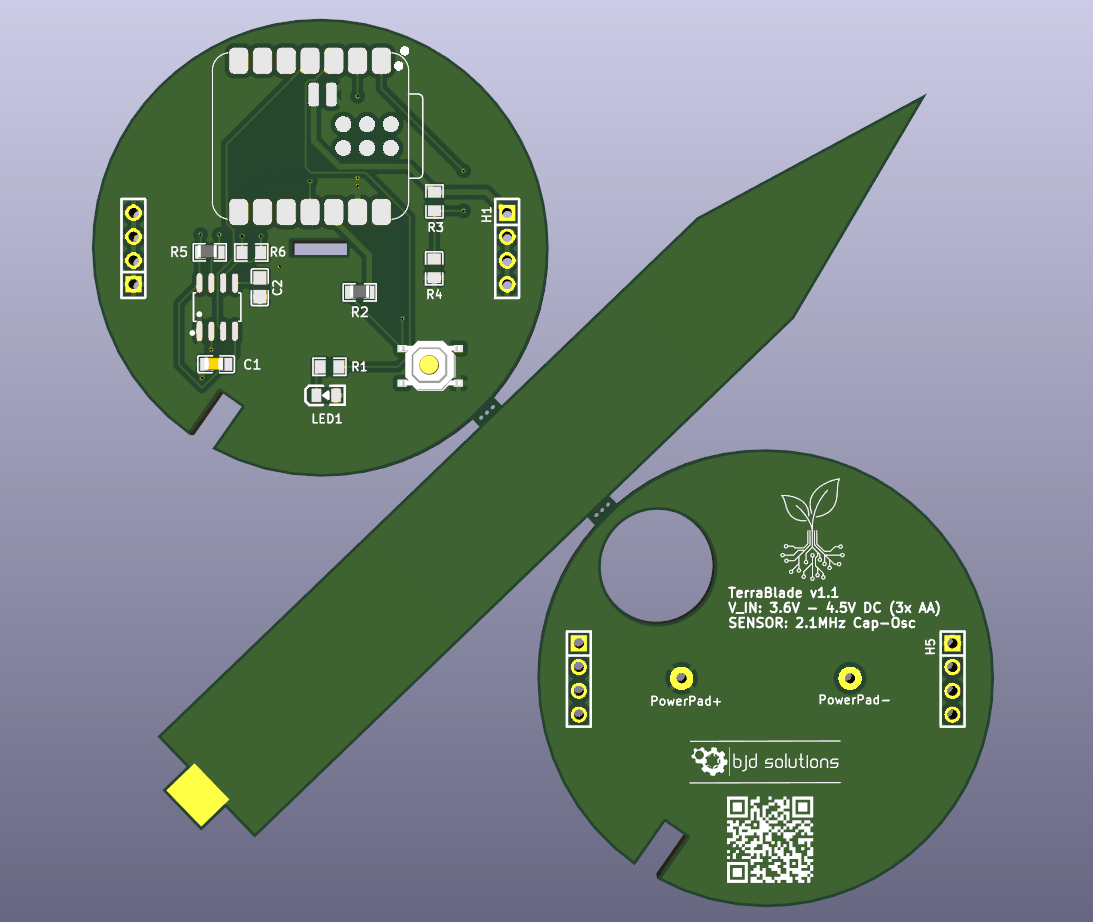
2 layers96.4 × 95 mmTerraBlade Sensor PCB, the printed circuit board in 3D

TerraBlade Sensor PCB

Ben-BJD/TerraBlade-Sensor-PCB3

TerraBlade is a professional-grade, ultra-low-power capacitive soil moisture sensor designed around the Seeed Studio XIAO ESP32-C3.

Size
96.4 × 95 mm
Copper layers
2
Thickness
1.6 mm
Parts
22
Nets
31
Pads
74
Tracks, vias
88, 14
Pours
6
Routed
Yes
KiCad
KiCad 9.0 (file 20241229)
Created
12 Apr 2026
Updated
2 Aug 2026

Overview

TerraBlade Sensor PCB is an open-source printed circuit board by Ben-BJD, from the Ben-BJD/TerraBlade-Sensor-PCB repository on GitHub. It is a 2-layer board of 96.4 × 95 mm with 22 parts on 31 nets, routed with 88 tracks and 14 vias.

It is built around the 2.54-1*4P母, TS-1187A-B-A-B and TZ-P2-0805YGTCS2-0.8T. Its parts include 6 resistors, 2 capacitors, 2 ICs, 2 connectors and 1 diode. It belongs with the sensors and measurement boards and the ESP32 and RISC-V boards of this library.

Main components

3

README

README.md

🌱 TerraBlade Sensor - Hardware PCB


Watch the Tutorial Read the Article

Project Available on PCBWay

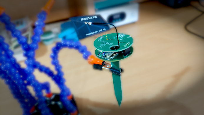
Assembled Board

TerraBlade 3D Render

TerraBlade is a professional-grade, ultra-low-power capacitive soil moisture sensor designed around the Seeed Studio XIAO ESP32-C3.

This repository contains the complete KiCad 9 hardware design files, manufacturing plots, and mechanical Inkscape references for the PCB assembly. This board is designed using a "PCBA-Driven" workflow, meaning the electronics were engineered first, acting as the structural core for a modular 3D-printed enclosure.

Created by BJD Solutions.


Key Engineering Features

  • True Digital Capacitive Sensing: Ditching the noisy, drifty analog peak-detectors of standard cheap soil sensors. The FR4 PCB blade acts as the timing capacitor for an industrial-grade TLC555IDR oscillator. It outputs a raw, clean frequency directly to the ESP32's hardware Pulse Counter (PCNT) for flawless, high-resolution moisture data.
  • Zero-Leakage "Parasitic" Power: The 555 timer is powered directly by an ESP32 GPIO pin. The ESP32 wakes up, powers the sensor, takes a reading, and kills the power before going back to sleep. Sensor quiescent current: 0.0µA.
  • Panelized 3-in-1 Design: The Radio PCB, Power Hat, and Sensor Blade are all designed to be manufactured on a single 100x100mm panel connected by mouse-bites to save on fabrication costs.
  • Mortise & Tenon Assembly: The Sensor Blade features a custom "tenon" tab that slots perfectly into the main Radio PCB and is soldered directly at a 90-degree angle, requiring zero wires.
  • Pogo-Pin Power Hat: Handles the mechanical shear force of a plunging outdoor sensor by using through-hole Pogo Pins (spring-loaded contacts) rather than weak SMD conical springs.
  • Low-Voltage Optimized: Features an ultra-efficient 573nm Yellow-Green LED that requires only ~2.0V to light up. It will reliably flash in "Config Mode" even when the 3x AA batteries are nearly dead. Includes a precision 1% 220kΩ voltage divider for highly accurate battery monitoring.

📂 Repository Structure

  • Full KiCad 9 project files (.kicad_pro, .kicad_sch, .kicad_pcb).
  • Ready-to-order plot files, drill files, and the solder paste stencil map.
  • High-resolution PDF exports of the schematic and PCB layers.
  • Original Inkscape (.svg) files used to perfectly calculate the complex Edge.Cuts curves, alignment notches, and Mortise & Tenon joints.

🛠️ Assembly & Manufacturing Notes

If you are ordering these boards from a fabricator please note the following:

  1. Thickness: Order in standard 1.6mm FR4. The Mortise and Tenon slot on the Radio PCB is routed to exactly 1.7mm to provide a perfect slip-fit for 1.6mm thick material.
  2. Solder Mask is Mandatory: Do NOT expose the copper on the Sensor Blade. The blade relies on the green Solder Mask to act as a waterproof dielectric barrier. Exposing the copper to wet soil will cause rapid galvanic corrosion and destroy the sensor.
  3. Keyway Notches: The Radio PCB and Power Hat feature an 8-o'clock alignment notch. This is an asymmetrical keyway designed to interface with a matching rail in the future 3D-printed enclosure, preventing the board from twisting or being inserted backward.
  4. Solder Paste Stencil: The F.Paste layer has been custom-tailored to remove paste from the structural Mortise & Tenon joints, allowing for clean, manual fillet soldering without bridging.

🛒 BOM Highlights (LCSC)

The full BOM is included and can be generated from the KiCad schematic, here are the critical components used in this design:

  • Microcontroller: Seeed Studio XIAO ESP32-C3
  • Timer IC: TLC555IDR (Industrial Temp Range: -40°C to 85°C) - LCSC: C6987
  • Pogo Pins (Power Contacts): CHIN-BAN PG1000-01-010P (1A Through-Hole) - LCSC: C49451494
  • Config LED: TUOZHAN 0805 Yellow-Green 573nm (1.8V-2.4V) - LCSC: C688885
  • Tactile Switch: TS-1187A-B-A-B (4-pin SMD) - LCSC: C318884

📄 License

This hardware design is open-source. Feel free to build it, mod it, and plant it! Designed by BJD Solutions.
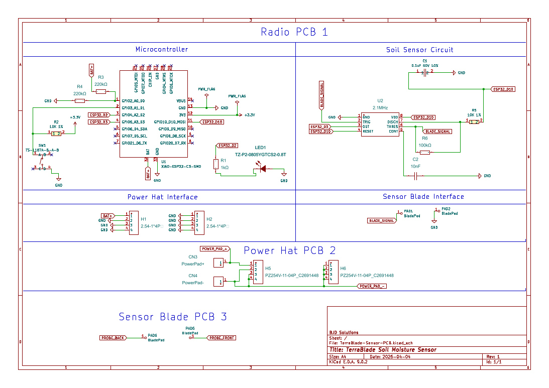

Schematic:

PDF Version

Board schematic

Parts

22
QtyValueFootprintReferences
4BladePadCustom:BladePad_SMDBLADE_SIGNAL, GND, PAD5, PAD6
210K 1%easyeda2kicad:R0805R2, R5
22.54-1*4P母Custom:HDR-TH_4P-P2.54-V-F+, H2
2220kΩCustom:R0805R3, R4
2PZ254V-11-04P_C2691448Custom:HDR-TH_4P-P2.54-V-M+, H6
10.1uF 50V 10%easyeda2kicad:C0805C1
1100kΩCustom:R0805R6
110nFCustom:C0805C2
11kΩCustom:R0805R1
12.1MHzCustom:SOIC-8_L4.9-W3.9-P1.27-LS6.0-BLU2
1PowerPad+Custom:TESTPOINT-SMD_BD2.0-D1.0-CustomCN3
1PowerPad-Custom:TESTPOINT-SMD_BD2.0-D1.0-CustomCN4
1TS-1187A-B-A-Beasyeda2kicad:SW-SMD_4P-L5.1-W5.1-P3.70-LS6.5-TL_H1.5SW1
1TZ-P2-0805YGTCS2-0.8TCustom:LED0805-R-RD_GREENLED1
1XIAO-ESP32-C3-SMDSEED:XIAO-ESP32-C3-SMDU1

Similar boards

  • 2 layers105 × 105 mmGW A, the printed circuit board in 3D

    GW A

    ayaxan7/SolarAlert

    SolarAlert is a compact embedded hardware project designed to monitor the health and performance of solar panels.

    97 parts
  • 2 layers120 × 50 mmOpengamma, the printed circuit board in 3D

    Opengamma

    Safecast/bGeigieScint

    The board features an integrated boost converter + linear regulator topology for SiPM bias generation:

    65 parts2
  • 2 layers95 × 60 mmSunrise alarm, the printed circuit board in 3D

    Sunrise alarm

    nicollsf/sunrise_alarm

    42 parts
  • 2 layers36.2 × 63.1 mmPicoMemcard pico, the printed circuit board in 3D

    PicoMemcard pico

    dangiu/PicoMemcard

    Emulating PSX Memory Card (or controller) using a Raspberry Pi Pico

    8 parts694GPL-3.0
  • 2 layers10.3 × 23.3 mmMini receiver, the printed circuit board in 3D

    Mini receiver

    loopj/wavephoenix

    Open-source implementation of the Nintendo WaveBird receiver using Silicon Labs Wireless Gecko SoCs

    11 parts430
  • 4 layers86 × 34 mmBsl drv v1, the printed circuit board in 3D

    Bsl drv v1

    jackw01/scanlight

    A better light source for scanning color negative film

    157 parts397CERN-OHL-W-2.0
  • 2 layers26.5 × 34.4 mmPicoLoaderNSB, the printed circuit board in 3D

    PicoLoaderNSB

    makeo/PicoLoader

    A cheap and easy to install modchip for the Nintendo GameCube!

    45 parts320GPL-2.0

Questions

How big is the TerraBlade Sensor PCB PCB?

It measures 96.4 × 95 mm and has 2 copper layers, 1.6 mm thick.

What parts does the TerraBlade Sensor PCB use?

22 parts, built around the 2.54-1*4P母, TS-1187A-B-A-B and TZ-P2-0805YGTCS2-0.8T. The full list of its parts is on this page, with links to each part's symbol and footprint where PCBKit's library has them.

Where can I download the TerraBlade Sensor PCB KiCad files?

From the Ben-BJD/TerraBlade-Sensor-PCB repository on GitHub, at the commit this page was made from: the board is TerraBlade-Sensor-PCB.kicad_pcb and its schematic TerraBlade-Sensor-PCB.kicad_sch. PCBKit opens the board in the browser, with nothing to install.

Can I use the TerraBlade Sensor PCB design in my own project?

Its repository states no licence, so its author keeps all rights: ask Ben-BJD before reusing the design.