2 layers34 × 96 mm
 Acidicts/MPad
Media-HackPad
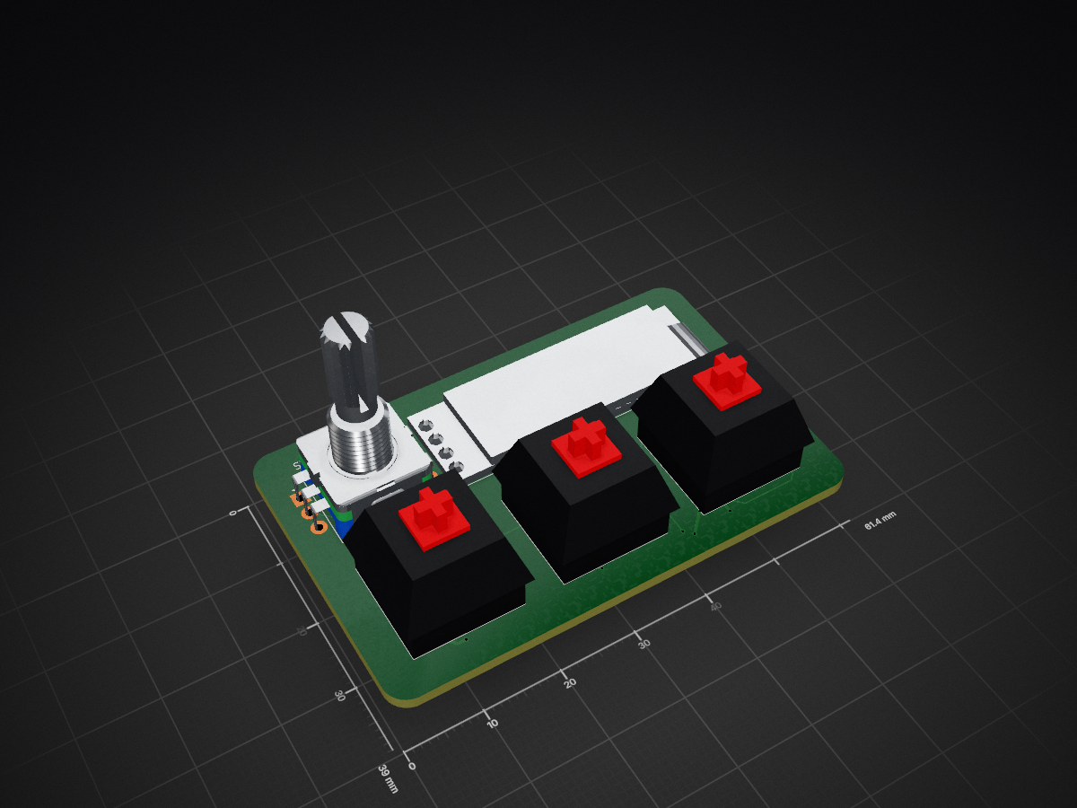
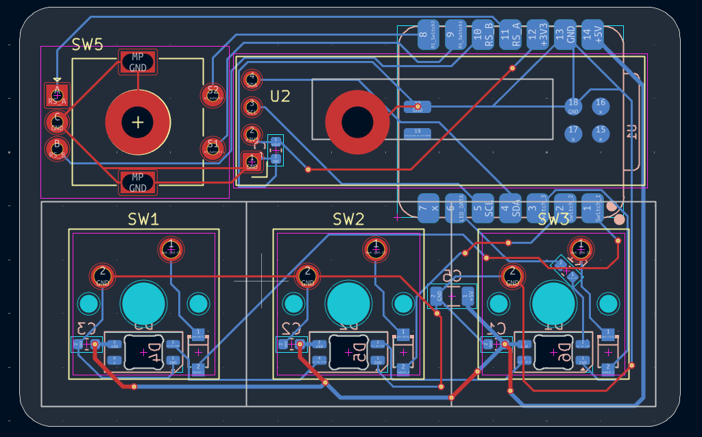
HackPad is an open-source printed circuit board by Acidicts, from the Acidicts/MPad repository on GitHub. It is a 2-layer board of 61.4 × 39 mm with 18 parts on 25 nets, routed with 182 tracks and 18 vias.
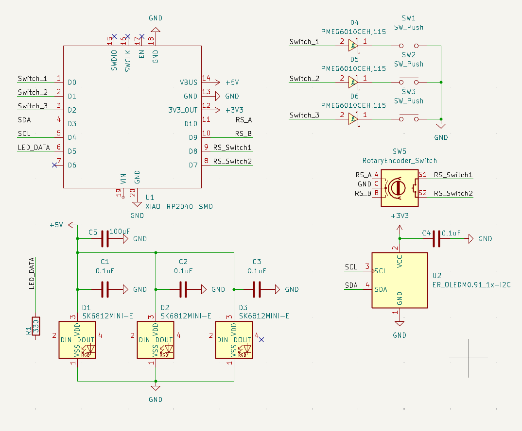
It is built around the PMEG6010CEH,115-JSM and SK6812MINI-E. Its parts include 6 diodes, 5 capacitors, 4 switches, 2 ICs and 1 resistor. It belongs with the RP2040 boards of this library.


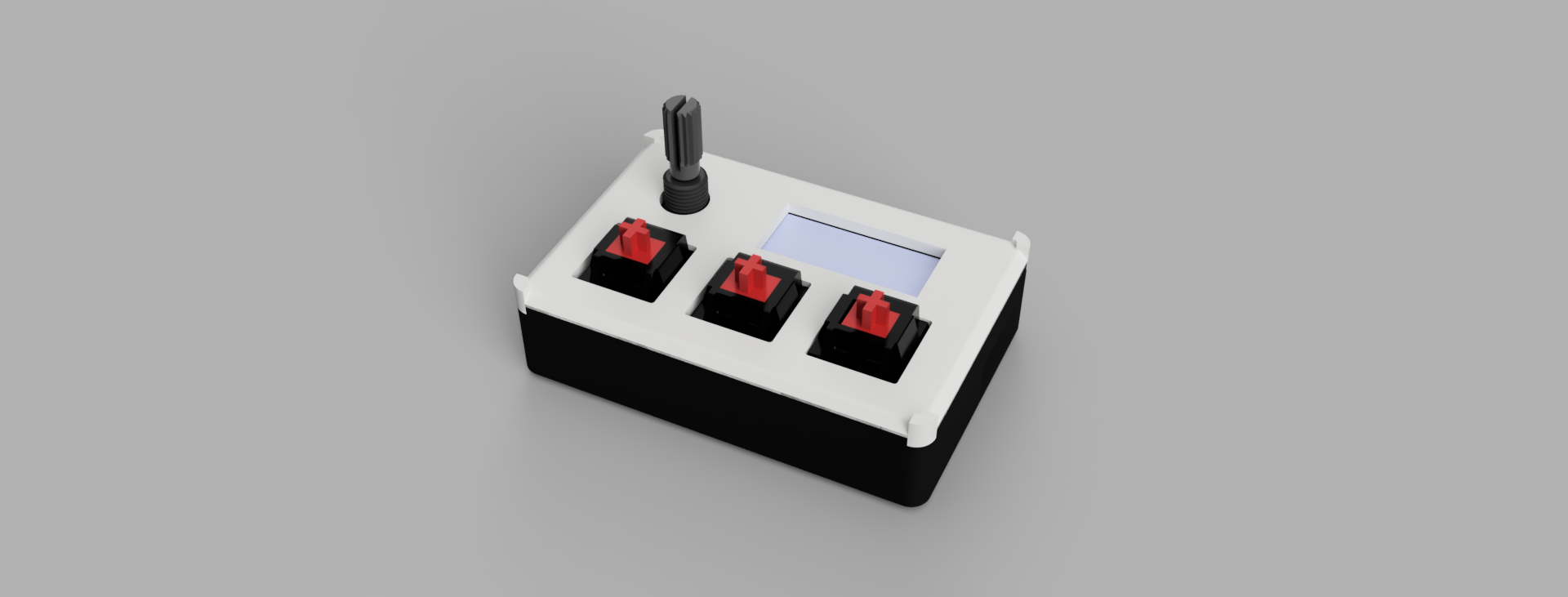
A Hackpad but this time made for media with 3 dedicated keys for Back, Play/Pause, and Skip along with volume controls via a rotary encoder. Powered by kmk on circuitpython
| Function | Key |
|---|---|
| Back | KC.WBAK |
| Play/Pause | KC.MPLY |
| Skip | KC.WFWD |
| Function | Key |
|---|---|
| Volume Down | KC.VOLD |
| Volume Up | KC.VOLU |
| Mute | KC.MUTE |
RPI-RP2.RPI-RP2 drive. The board will reboot and show up as a USB drive called CIRCUITPY.firmware folder onto the CIRCUITPY drive.~ Note It is configured for getting stock prices edit the firmware to do as you see fit ~ It uses main.py on the host to communicate over serial
~ Note the capacitors and resistors on the pcb are optional, as they are for decoupling and filtering
CIRCUITPY.| Qty | Value | Footprint | References |
|---|---|---|---|
| 4 | 0.1uF | Capacitor_SMD:C_0603_1608Metric | C1, C2, C3, C4 |
| 3 | PMEG6010CEH,115 | easyeda2kicad:SOD-123FL_L2.7-W1.8-LS3.8-RD | D4, D5, D6 |
| 3 | SK6812MINI-E | LED_SMD:LED_SK6812MINI-E_3.2x2.8mm_P1.5mm_ReverseMount | D1, D2, D3 |
| 3 | SW_Push | Button_Switch_Keyboard:SW_Cherry_MX_1.00u_PCB | SW1, SW2, SW3 |
| 1 | 100uF | Capacitor_SMD:C_1206_3216Metric | C5 |
| 1 | 330 | Capacitor_SMD:C_0603_1608Metric | R1 |
| 1 | ER_OLEDM0.91_1x-I2C | Display:ER_OLEDM0.91_1x-I2C | U2 |
| 1 | RotaryEncoder_Switch | Rotary_Encoder:RotaryEncoder_Alps_EC11E-Switch_Vertical_H20mm | SW5 |
| 1 | XIAO-RP2040-SMD | OPL:XIAO-RP2040-SMD | U1 |

marklynch/pool-controller-pcb
PCB Design files for pool controller for Connect 10

balu-16/SeedGrant_Safety
Personal-safety project: Expo / React Native client + FastAPI + PostgreSQL (Supabase) backend + React admin portal.

Wireb/Train_lighting_card
PCB and firmware for model train automotive lighting control card. MIT licence

embeddedos-org/eCAD-Hardware-Products
Hardware designs + EE docs + Board datasheets of Multiple products

Digital-Naturalism-Laboratories/Mothbox_Electronics
This is where the electronics for the Mothbox are developed, such as the PCB! It's copied over from https://github.com/Digital-Naturalism-Laboratories/Mothbox/tree/main/Hardware/PCB so you can check that out if you want…

stockmann-lab/shim_amp_hardware_linear
Hardware related to open-source shim amplifier development for MRI research

DeadlySIn777/Controller
Unfinished CNC controller motherboard: native KiCad sources, rules, DSN and global routing review
It measures 61.4 × 39 mm and has 2 copper layers, 1.6 mm thick.
18 parts, built around the PMEG6010CEH,115-JSM and SK6812MINI-E. The full list of its parts is on this page, with links to each part's symbol and footprint where PCBKit's library has them.
From the Acidicts/MPad repository on GitHub, at the commit this page was made from: the board is kicad/HackPad.kicad_pcb and its schematic kicad/HackPad.kicad_sch. PCBKit opens the board in the browser, with nothing to install.
Its repository states no licence, so its author keeps all rights: ask Acidicts before reusing the design.