2 layers17.8 × 33 mm

 74th/ch32v-dev-boards11
Wchlinke swd adapter checker is an open-source printed circuit board by 74th, from the 74th/ch32v-dev-boards repository on GitHub, published under the MIT licence. It is a 2-layer board of 52 × 50 mm with 59 parts on 62 nets, routed with 269 tracks and 66 vias.
Its parts include 20 resistors, 20 diodes, 10 transistors, 2 capacitors and 1 IC. It belongs with the interfaces and adapters boards and the RISC-V boards of this library.
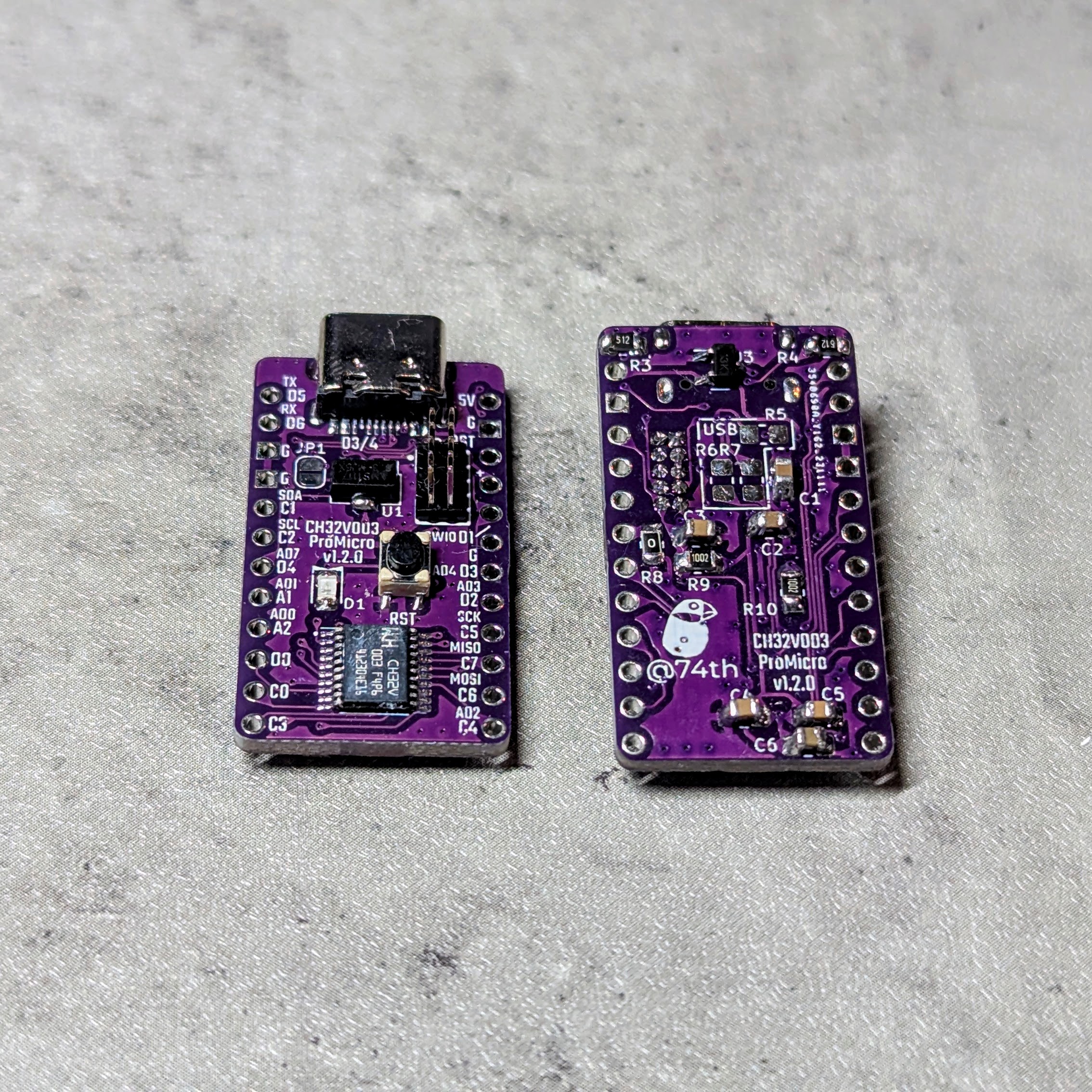
Shop(Booth, Japan): https://booth.pm/ja/items/4645948
🇯🇵
🇯🇵
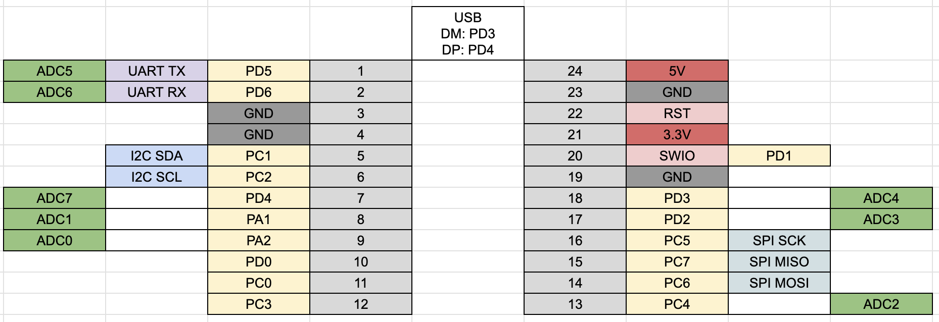
| Reference | Name | Quantity |
|---|---|---|
| C1, C2 | Capacitor 0805 10uF | 2 |
| C3-C5 | Capacitor 0805 100nF | 3 |
| C6 | Capacitor 0805 1uF | 1 |
| D1 | LED 0805 Blue | 1 |
| J1 | USB Type-C Receptacle | 1 |
| J2 | Pin Header 2x5 Pitch 1.27mm | 1 |
| JP1 | Jumper SolderJumper_2_Open | 1 |
| R3, R4 | Register 0805 5.1kΩ | 2 |
| R5 | Register 0805 1.5kΩ (NC) | 1 |
| R6, R7 | Register 0805 27.4Ω (NC) | 2 |
| R8 | Register 0805 0Ω | 1 |
| R9, R10 | Register 0805 10kΩ | 2 |
| SW1 | Button SKRPABE010 | 1 |
| U1 | Regulator 3.3V SOT-89 AMS1117-3.3 | 1 |
| U2 | MCU TSSOP20 WCH CH32V003F4P6 | 1 |
🇯🇵
| Reference | Name | Quantity |
|---|---|---|
| C1, C2 | Capacitor 0805 10uF | 2 |
| C3-C5 | Capacitor 0805 100nF | 3 |
| C6 | Capacitor 0805 1uF | 1 |
| D1 | LED 0805 Blue | 1 |
| J1 | USB Type-C Receptacle - USB2.0_C_v3 | 1 |
| J2 | Box Pin Header 2x5 Pitch 1.27mm | 1 |
| JP1 | Jumper SolderJumper_2_Open | 1 |
| R1, R9, R10 | Register 0805 10kΩ | 3 |
| R2 | Register 0805 54-56kΩ | 1 |
| R3, R4 | Register 0805 5.1kΩ | 2 |
| R5 | Register 0805 1.5kΩ (NC) | 1 |
| R6, R7 | Register 0805 27.4Ω (NC) | 2 |
| R8 | Register 0805 0Ω | 1 |
| SW1 | Button SKRPABE010 | 1 |
| U1 | Regulator 3.3V SOT-89 AMS1117-3.3 | 1 |
| U2 | MCU TSSOP20 WCH CH32V003F4P6 | 1 |
| U3 | USB Power Protection IC SOT-23-6L CH217K | 1 |
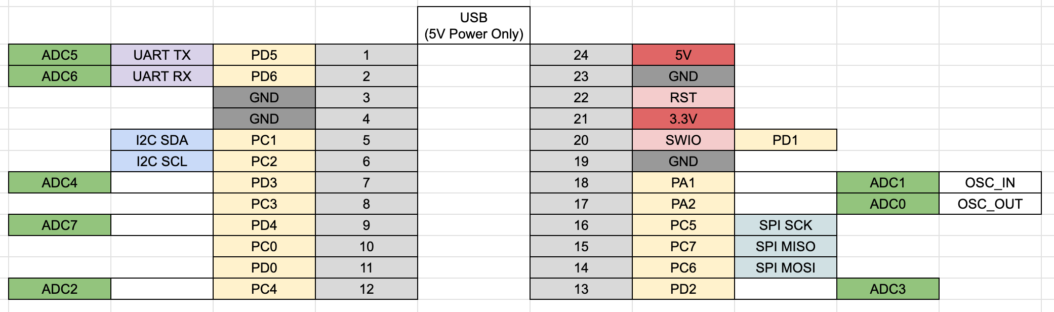
| Reference | Parts |
|---|---|
| R1 | 0805 Register 10k |
| R2,R3 | 0805 Register 5.1kR |
| R4 | 0805 Register 200R or 1kR |
| R5 | 0805 Register 0R |
| C1,C2,C3 | 0805 Capacitor 100nF |
| C4,C5 | 0805 Capacitor 22p (NC) |
| C6 | 0805 Capacitor 10uF |
| C7 | 0805 Capacitor 2.2uF |
| D1 | 0805 LED |
| U1 | TSSOP20 CH32V003F4P6 |
| U2 | SOT89 3.3V Regulator AMS1117-3.3 |
| Y1 | 3225 4Pin Crystal 24MHz (NC) |
| J1 | SMD USB-C 2.0 Socket |
| SW1 | SKRPABE010 SMD Push Switch |
| Qty | Value | Footprint | References |
|---|---|---|---|
| 20 | 10k | 74th:Register_0805_2012 | R1, R2, R3, R4, R5, R10, R11, R12, R13, R14, R15, R16, R17, R18, R19, R20 +4 |
| 20 | BLUE | 74th:LED_0805_2012 | D1, D2, D3, D4, D5, D10, D11, D12, D13, D14, D15, D16, D17, D18, D19, D20 +4 |
| 10 | 2N7002 | Package_TO_SOT_SMD:SOT-23 | Q1, Q2, Q3, Q4, Q5, Q6, Q7, Q8, Q9, Q10 |
| 2 | BoxPinHeader2x5 | 74th:Connector_BoxPinHeader_2x05_P1.27mm | CH1, CH4 |
| 1 | 100n | 74th:Capacitor_0805_2012 | C2 |
| 1 | 10u | 74th:Capacitor_0805_2012 | C1 |
| 1 | Battery_Cell | 74th:BatteryHolder-CR2032 | BT1 |
| 1 | CH32V002F4P6 | 74th:Package_TSSOP-20_4.4x6.5mm_P0.65mm | U1 |
| 1 | PinHeader2x5 | 74th:PinOut_Pin_2x5_1GND | CH2 |
| 1 | SWD | 74th:PinOut_Pin_3_3GND | CH3 |
| 1 | SW_Slide | 74th:Switch_Slide_SK-12D02-G020 | SW1 |


davidphilipbarr/Sweep
Sweep - a small promicro based keyboard inspired by the Ferris.


VoronDesign/Voron-Hardware
Cool Hardware designed by the Voron Design group


dmcke5/NucDeck
The Open Source DIY Handheld Gaming PC!

jackw01/scanlight
A better light source for scanning color negative film

ChrisChrisLoLo/beyblock20
The magnetic, modular, 20-key macropad that can join together to form an ortholinear board

sadekbaroudi/vik
This is a VIK module designed to mount a PER56 scroll ring, with a 35mm Cirque Trackpad and optional WS2812B LEDs.
It measures 52 × 50 mm and has 2 copper layers, 1.6 mm thick.
59 parts. The full list of its parts is on this page, with links to each part's symbol and footprint where PCBKit's library has them.
From the 74th/ch32v-dev-boards repository on GitHub, at the commit this page was made from: the board is wchlinke-swd-adapter/wchlinke-swd-adapter-checker/wchlinke-swd-adapter-checker.kicad_pcb and its schematic ch32v003-promicro/ch32v003-promicro.kicad_sch. PCBKit opens the board in the browser, with nothing to install.
Its repository publishes it under the MIT licence: you may reuse it on that licence's terms (keep the author's notice, and for a copyleft licence share your changes alike).