2 layers35 × 50 mm
 74th/switch-dip
自作キーボードのスイッチをユニバーサル基板でも使うための変換基板
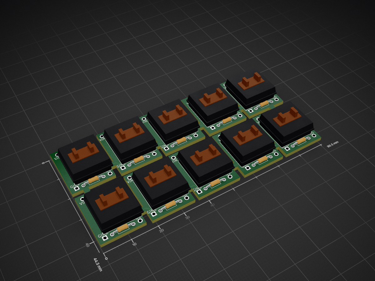
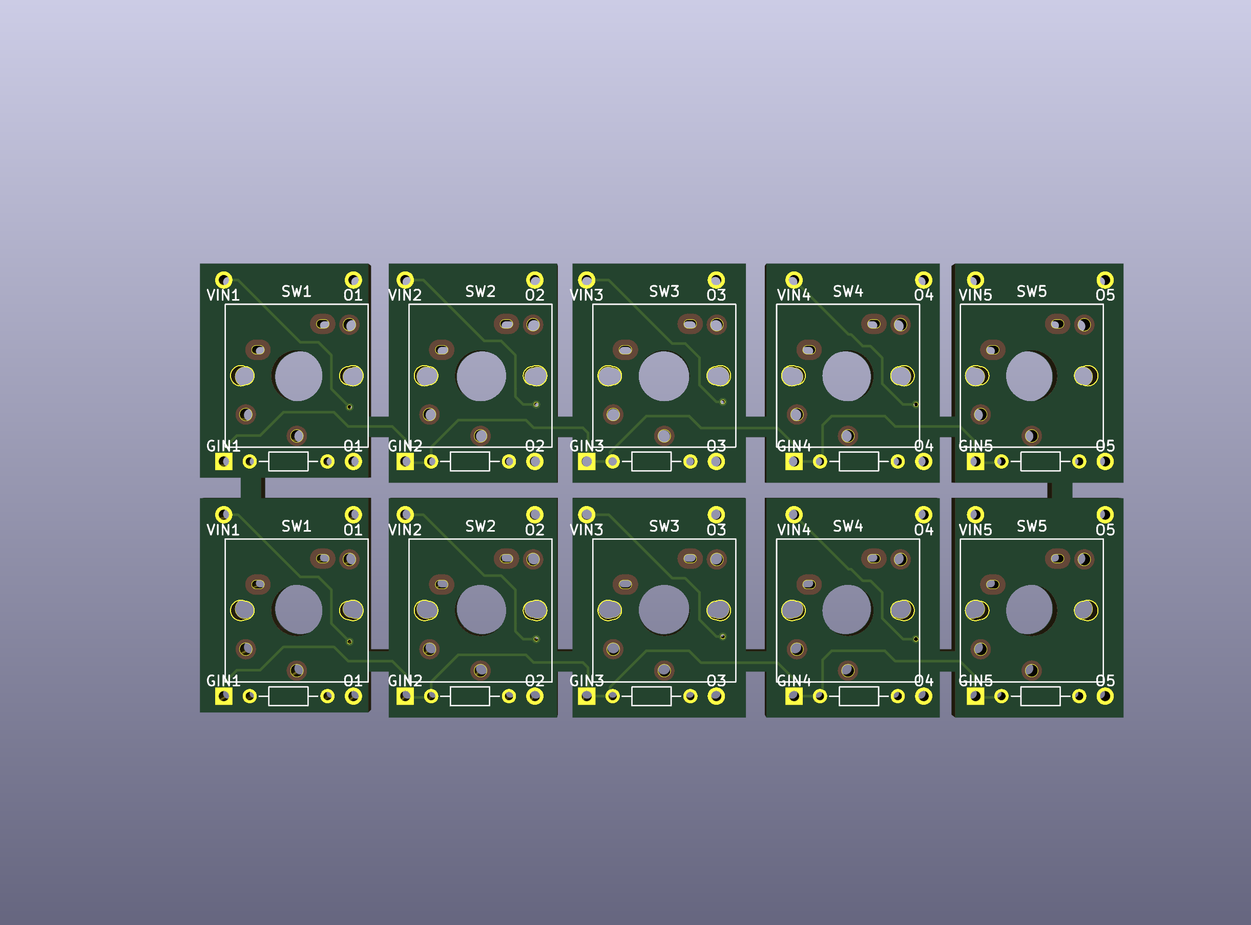
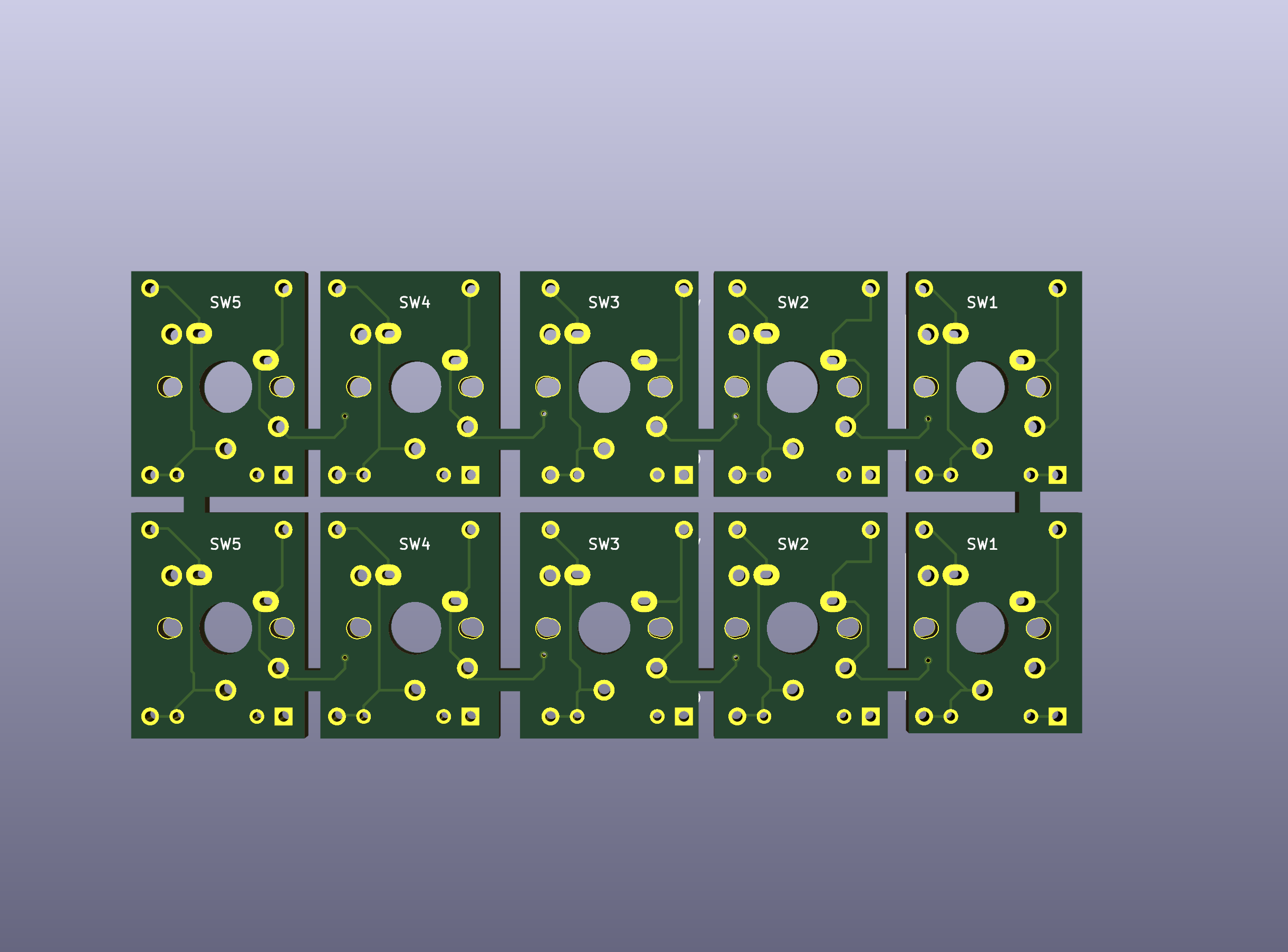
Switch dip is an open-source printed circuit board by 74th, from the 74th/switch-dip repository on GitHub. It is a 2-layer board of 90.5 × 44.5 mm with 60 parts on 7 nets, routed with 364 tracks and 8 vias.
Its parts include 10 resistors and 10 switches.
CC BY 4.0 [blocked]
| Qty | Value | Footprint | References |
|---|---|---|---|
| 20 | OUTPUT | $switch-dip:Pin_circle | O1, O1, O1, O1, O2, O2, O2, O2, O3, O3, O3, O3, O4, O4, O4, O4 +4 |
| 10 | GIN | $switch-dip:Pin_rect | GIN1, GIN1, GIN2, GIN2, GIN3, GIN3, GIN4, GIN4, GIN5, GIN5 |
| 10 | R | $switch-dip:Register | R1, R1, R2, R2, R3, R3, R4, R4, R5, R5 |
| 10 | SW_PUSH | $switch-dip:CherryMX_Choc_1u | SW1, SW1, SW2, SW2, SW3, SW3, SW4, SW4, SW5, SW5 |
| 10 | VIN | $switch-dip:Pin_circle | VIN1, VIN1, VIN2, VIN2, VIN3, VIN3, VIN4, VIN4, VIN5, VIN5 |
It measures 90.5 × 44.5 mm and has 2 copper layers, 1.6 mm thick.
60 parts. The full list of its parts is on this page, with links to each part's symbol and footprint where PCBKit's library has them.
From the 74th/switch-dip repository on GitHub, at the commit this page was made from: the board is switch-dip.kicad_pcb. PCBKit opens the board in the browser, with nothing to install.
Its repository states no licence, so its author keeps all rights: ask 74th before reusing the design.


sd2psx/pcb
The PCB must be produced in 0.8mm thickness. Production files are provided under the "Releases" tab. These do not include the through-hole OLED module.


BitDogLab/BitDogLab
Open-source educational hardware for embedded systems, programming, electronics, and physical computing.