2 layers299.2 × 180 mm

 256byteram/6530-Replacement7
Replaces the 6530 ICs found on Allied Leisure pinball machines.
6530 to 6532 adaptor is an open-source printed circuit board by 256byteram, from the 256byteram/6530-Replacement repository on GitHub, published under the GPL-3.0 licence. It is a 2-layer board of 100.3 × 100.3 mm with 29 parts on 125 nets, routed with 651 tracks and 72 vias.
It is built around the 74LS42PC, 74LS00SC and 74LS11DC. Its parts include 7 ICs, 6 capacitors, 6 diodes, 5 connectors and 3 resistors.


Replaces the 6530 ICs found on early revision Allied Leisure pinball machines.
Please note these designs and instructions come with absolutely no warranty, implied or otherwise. I write these instructions assuming the builder has experience in assembling electronics.
You will need:
x1 27C64 EPROM (or equivalent)
x1 28 pin DIP IC socket
x2 6532 IC's
x5 40 pin IC socket - Dual wipe, not machined
x1 74LS42 DIP IC
x1 16 pin DIP IC socket
x1 74LS11 DIP IC
x2 74LS00 DIP IC
x3 14 pin DIP IC socket
x6 1N4148 silicon diodes
x1 2N7000 transistor
x3 1k ohm 1/4W resistors
x1 1k x6 resistor network (or alternatively an additional 6 1k ohm 1/4W resistors)
x6 100nF 50V monolithic capacitors
x100 pin headers to fit the original sockets on the CPU board (5 rows of 20 pins)
Alternatively: x5 stackable headers for the ESP32 Sparkfun part number PRT-14311. These won't damage IC sockets. See Construction Notes below.
To have these boards manufactured, it should be as simple as zipping the 6530-Replacement-Gerber folder and submitting them to a PCB manufacturer. The board dimensions are 100.3 x 100.3mm
I can not host the ROM image here as they are copyrighted. I have supplied a 1k blank image to assist with generating the required ROM image.
There are three ROM binaries I was supplied with, one each from the three original 6530's:
EE1712_82219_DG_MOS6530_009.bin
EE1712_82219_DG_MOS6530_010.bin
EE1712_82219_DG_MOS6530_011.bin
To generate a ROM binary for the board on Linux or Mac in the terminal:
cat Blank1k.bin Blank1k.bin Blank1k.bin EE1712_82219_DG_MOS6530_009.bin Blank1k.bin EE1712_82219_DG_MOS6530_010.bin EE1712_82219_DG_MOS6530_011.bin Blank1k.bin > AdaptorROM.bin
And on the Windows command prompt:
copy /b Blank1k.bin+Blank1k.bin+Blank1k.bin+EE1712_82219_DG_MOS6530_009.bin+Blank1k.bin+EE1712_82219_DG_MOS6530_010.bin+EE1712_82219_DG_MOS6530_011.bin+Blank1k.bin AdaptorROM.bin
You will first need to cd to the directory the ROMs are in. This will give you an 8kB ROM image ready to burn to a 27C64 or equivalent EPROM.
To use a 27C256 or similar EPROM join pins 26 and 27 together on U8 of the Replacement board (the EPROM) with some solder.
To generate the required binary, create the AdaptorROM.bin file as previously instructed, then:
cat AdaptorROM.bin AdaptorROM.bin AdaptorROM.bin AdaptorROM.bin > AdaptorROM32k.bin
or on Windows:
copy /b AdaptorROM.bin+AdaptorROM.bin+AdaptorROM.bin+AdaptorROM.bin AdaptorROM32k.bin
I recommend first replacing, at minimum, the three original 6530 IC sockets on the main board with dual wipe sockets. Do not use machined sockets. Ideally, all sockets should be replaced.
The headers need to be installed before the IC sockets on the Replacement board are installed.
If you are using ESP32 stackable headers, they won't damage the IC sockets on the main board, however they are more complicated to solder. Install all headers in the board from the component side, then flip the board so the black housings of the headers are on a flat surface. They will align themselves vertically. They can now be soldered. It will be easier if each header has one pin soldered first to keep it from moving.
When the pins are soldered, the black housing of the headers can be removed with a small pair of pliers. Once the housing starts to move it will release easily. The pins remaining where the housing was removed can be cut off. You should be left with the pins on the solder side of the board.
If you are using regular pin headers, they will tend to damage the IC sockets on the main board. I recommend replacing the original sockets with new dual wipe sockets. Do not use machined IC sockets. They need to be installed from the solder side of the board and soldered on the component side. Make sure the pins are aligned vertically. Solder one pin in place, then melt the solder again while aligning the header. The header won't move after the solder has cooled.
Construction from then on should be straight forward, following the usual rules.
If you are using a resistor network for RN1, the dot needs to align with the square pad.
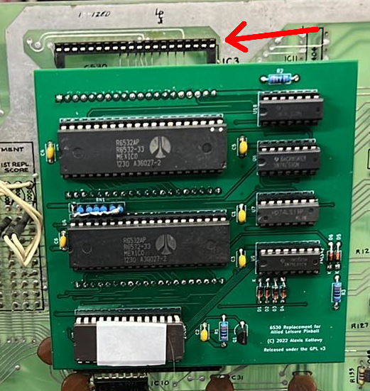
Installing the board has several issues which need to be considered. The main one is confusion over how it plugs into the sockets on the main board. The top row of the IC3 socket - pins 21 through 40 - should not connect to anything. All other pins should line up with the sockets. Check and re-check alignment before inserting the board.
If you are using CMOS variant MC6821 GPIO chips, you will need to install pull-up resistors to the following pins and +5V:
IC1 - Pins 2-9
IC4 - Pins 2-5, 19
IC7 - Pins 2-9, 39, 40
IC8 - Pins 18, 19, 39, 40
This is because the original MOS 6520's would naturally float to a logic high. The MC6821's do not, instead they pick up any noise. The machine will not run without these resistors.
Please do not modify your board if there are no bodge wires, as it is the newer revision. This information is provided as a reference for early revision boards that needed the modifications. They are as follows:
IC4:
IC8:
Pin 10 -> IC29 pins 10, 9
Pin 11 -> IC40 pin 1
Pin 12 -> IC40 pin 2
Pin 13 -> IC40 pin 4
Pin 14 -> IC40 pin 5
IC29:
Pins 1, 2 -> J2-W (originally wired to IC4 pin 28)
Pin 3 -> Pin 5
Pin 4 -> IC40 pin 6
Pin 8 -> IC40 pin 3
The following traces are cut:
IC4:
Pin 9 -> J1 (cut near J1)
Pin 18 (cut near pin and on trace near J2)
Pin 19 (cut near pin)
IC29:
Pins 1, 2 -> IC40 pin 2
Pin 5 -> IC40 pin 1
Pin 13 -> IC40 pin 3 (cut near via)
1N4007 diodes should be installed in all resistor locations near J2 and J3. The anode (not striped) should connect to 6V/24V GND in the middle of the array, i.e. the diodes should be pointing away from ground and to the signals.
Good luck!
| Qty | Value | Footprint | References |
|---|---|---|---|
| 6 | 100n | Capacitor_THT:C_Disc_D5.0mm_W2.5mm_P5.00mm | C1, C2, C3, C4, C5, C6 |
| 6 | 1N4148 | Diode_THT:D_DO-34_SOD68_P7.62mm_Horizontal | D1, D2, D3, D4, D5, D6 |
| 3 | 1k | Resistor_THT:R_Axial_DIN0207_L6.3mm_D2.5mm_P10.16mm_Horizontal | R1, R2, R3 |
| 2 | 6532 | Package_DIP:DIP-40_W15.24mm_Socket_LongPads | U2, U4 |
| 2 | 74LS00 | Package_DIP:DIP-14_W7.62mm_Socket_LongPads | U6, U10 |
| 2 | IC5 | Connector_PinHeader_2.54mm:PinHeader_1x20_P2.54mm_Vertical | J1, J2 |
| 2 | IC6 | Connector_PinHeader_2.54mm:PinHeader_1x20_P2.54mm_Vertical | J4, J5 |
| 1 | 27C64 | Package_DIP:DIP-28_W15.24mm_Socket_LongPads | U8 |
| 1 | 2N7000 | Package_TO_SOT_THT:TO-92L_Inline_Wide | Q1 |
| 1 | 74LS11 | Package_DIP:DIP-14_W7.62mm_Socket_LongPads | U7 |
| 1 | 74LS42 | Package_DIP:DIP-16_W7.62mm_Socket_LongPads | U9 |
| 1 | IC3 | Connector_PinHeader_2.54mm:PinHeader_1x20_P2.54mm_Vertical | J3 |
| 1 | R_Network06 | Resistor_THT:R_Array_SIP7 | RN1 |
It measures 100.3 × 100.3 mm and has 2 copper layers, 1.6 mm thick.
29 parts, built around the 74LS42PC, 74LS00SC and 74LS11DC. The full list of its parts is on this page, with links to each part's symbol and footprint where PCBKit's library has them.
From the 256byteram/6530-Replacement repository on GitHub, at the commit this page was made from: the board is 6530 to 6532 adaptor.kicad_pcb and its schematic 6530 to 6532 adaptor.kicad_sch. PCBKit opens the board in the browser, with nothing to install.
Its repository publishes it under the GPL-3.0 licence: you may reuse it on that licence's terms (keep the author's notice, and for a copyleft licence share your changes alike).

ceteras/Cobra-XP
Derived from Cobra, an experimental board for testing all kind of mods.


abzman/intellivision-t-card
replica of the t-card development cart for the intellivision that takes standard ROMs

